FIELD GUIDESource-led reference

P198 / Storage / Connector

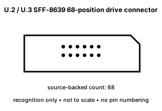
U.2 / U.3 SFF-8639 68-position drive connector

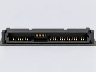
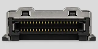
U.2/U.3 drive connectors use the SFF-8639 interface family; the cited connector series has 68 positions.

Also called U.2 U.3 SFF-8639 68 pin U.2

A shared drive-edge family does not mean every host, backplane and drive supports the same transport mode.

Look for

Verify U.2 versus U.3 support and the host/backplane protocol path before selecting a cable or drive.

Claim inspection dates: 2026-10-05, 2026-10-13 · Independent review pending

Image inspection / P198

See the view. Check its scope.

2 registered views for this reference. Different part examples are not automatically mates; all remain not to scale and independently unapproved.

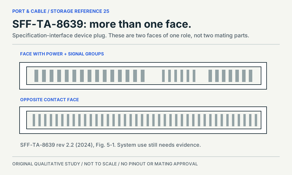
Additional contact regions distinguish the specification interface, not the system protocol. Specification-level device plug; an original source-observed qualitative study, not a pinout or safe-mating guide. (private workspace)

P198 / Source-observed physical study

SFF-TA-8639 / U.2–U.3 context

SFF-TA-8639 revision 2.2 device plug

Two contact-bearing faces of the specification device plug · Other declared component

Not to scale. Technical and rights review pending.

Inspect view & provenance (private workspace)
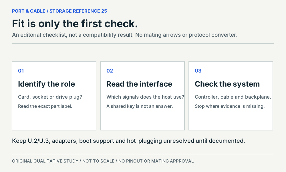
Editorial checklist separating storage component role, host interface and full system evidence. Not a physical specimen or a compatibility verdict. (private workspace)

P198 / Concept — not physical geometry

Storage: role, interface, system

Editorial evidence checklist; no physical component

Editorial checklist; no component view · Concept only

Not to scale. Technical and rights review pending.

Inspect view & provenance (private workspace)

The useful distinction

Recognize it. Then verify it.

U.2/U.3 drive connectors use the SFF-8639 interface family; the cited connector series has 68 positions. [C198A]

SFF-TA-8639 revision 2.2 defines a 68-contact system, while SFF-9639 explains that a device plug may populate only the contacts required by its use case. [C198B]

The device plug in SFF-TA-8639 Figure 5-1 has contact areas on opposite faces and additional fine-contact regions; one front-facing photograph cannot show the whole interface. [C198C]

SFF-TA-8639 revision 2.2 section 5.2 says its fixed-connector footprint is not generally a replacement for SFF-8482 or SFF-8630 footprints. [C198D]

SFF-9639 revision 2.2 is informational and directs readers to the using-interface standards for definitive signal definitions; it warns that its own tables may become inaccurate. [C198E]

Source-scoped identification facts

Each value retains its exact example, role and measurement axis. Facts from different parts must not be combined into an invented component.

Documented examples; not a mating drawing or compatibility approval
Nominal contacts68S202Source-backed position count for the cited U.2/U.3 series; not a signal map.
Positions / cavity span68 (Claim C198A)S202Recorded source-scoped values; named examples do not describe every family variant or establish compatibility. V36 catalogue-expansion identification fact only; not independent technical approval, fabrication data, wiring instruction or end-to-end compatibility proof.
Contact pitch0.8 mm additional opposite-side contact set described insection5.4S599Named source examples retain separate role, part, view and axis limits; values are not a universal family specification. SFF-8639 Rev2.2 connector interface. Full34-page current official specification is Rev2.2 May6,2024.68positions total, not all necessarily populated. Additional-contact pitch does not replace the separate inheritedSATA/SAS sections.
View conventionPublished receptacle and plug views remain distinct; termination-side numbering requires mating-side gender.S599Named source examples retain separate role, part, view and axis limits; values are not a universal family specification. SFF-8639 Rev2.2 connector interface. Full34-page current official specification is Rev2.2 May6,2024.68positions total, not all necessarily populated. Additional-contact pitch does not replace the separate inheritedSATA/SAS sections.

Not recorded: Populated contacts, Contact rows, Dimensions / axis, Connector role, Contact gender / arrangement, Mounting, Coupling / latch, Keying / polarization, Shell / form, Manufacturer, Series, Exact part / implementation, Recorded markings. Unknown fields stay unknown; illustrations supply no measurements or pin assignments.

Recorded variant and source limits
  • Check the exact device manual before wiring or applying power.
  • Wilder PCIe Gen-5 U.2 Plug (CLB) test fixture: Table 5 plug identifiers. Names use host direction; this fixture table includes mode-dependent sidebands.
  • SNIA SFF-TA-1001 U.3 PCIe device plug, single port: Device Plug / PCIe columns, Tables 4-1..4-3. Signal names from host perspective as explicitly stated on p.13.
  • U.2 / Quad PCIe plug — SNIA reference-guide use: Device plug numbers; PCIe PET/PER names are from the host perspective (Table 5-2 note), even on the device. Physical view follows SFF-8639 device-plug drawing.
  • U.3 / SFF-TA-1001 universal host receptacle: Use the separate host-receptacle/device-plug columns. PET/PER on a device still use host-perspective naming; E6 and S15 differ between host and device.
  • U.3 / SFF-TA-1001 PCIe device plug: Use the separate host-receptacle/device-plug columns. PET/PER on a device still use host-perspective naming; E6 and S15 differ between host and device.
  • Seagate Nytro 5060 2.5-inch U.2 device (named model family): Device manual Table 23 contact numbers. SG1/SG2 are separate ground features and are not counted among the 68 P/S/E contacts.
Report a correction to these facts →

Bounded facts, visible unknowns

Specifications and limits

U.2 / U.3 SFF-8639 68-position drive connector facts and limitations
Documented identification68-position U.2/U.3 SFF-8639 connector-series form. [C198A]
Source-scoped role and recognitionA common connector is not a common system. Additional contact regions distinguish the specification interface, not the system protocol. [C198B] [C198C] [C198D] [C198E]
Mechanical dimensionsNo independently reviewed mechanical drawing in V36; do not use this page for fabrication, fit testing or tolerance work.
Engineering pinoutSource-checked engineering profile available; independent review pending. Open engineering profile →
Verified device listNot included. Check exact device and accessory documentation.
A boundary, not an omission to guess around.

Use the source-backed form or position count only for identification. Resolve ratings, protocol, direction, wiring, cable construction and exact device support from the relevant equipment and component documentation.

Before you connect

What to check

  1. Identify the exact connector family and variant from the equipment or cable documentation.
  2. Keep shape, contact count, protocol, electrical rating and device support as separate facts.
  3. Do not force, rewire or adapt a connector from this recognition record; resolve the remaining requirements first.
Trace a supported connection class →

Pins & wiring

Pinout

Choose the exact wiring. Pin numbers follow its stated view; a schematic does not establish physical positions. Check your exact device before wiring.

What the status labels mean
Confirmed
Recorded research passes agree within this variant; this is not independent human review or hardware validation.
Single source
Only one underlying document, or one pass, supports this assignment.
Device-specific
Supported for the named equipment or wiring only. Check your device’s manual.
Unverified
Missing or conflicting evidence. Do not wire from this row.
Not connected
The source explicitly says NC, no contact or no pin for this wiring.
Wiring variant

Wilder PCIe Gen-5 U.2 Plug (CLB) test fixture

Device-specific wiring. Check your device’s manual before connecting or applying power.

View and evidence limits

Table 5 plug identifiers. Names use host direction; this fixture table includes mode-dependent sidebands.

  • P198 U.2 / U.3 — **Agree** on comparable PCIe lane placement; **partial for sidebands/modes** — Both read **the same SFF-TA-1001 rev 1.1 and SFF-9639 rev 2.2 documents**, with matching hashes. U.3 PCIe-device assignments and the same 11 blank cells agree. U.2 puts lane 0 on E10/E11/E13/E14 and lane 3 on E17/E18/E20/E21; U.3 relocates PCIe lanes to S2-S27. A adds Wilder's U.2 test fixture; B adds Seagate Nytro 5060 and a separate U.3 universal-host column. Host/device E6 and S15, reserved versus fixture-defined HPT roles, and unused power/legacy-data contacts remain variant-specific. Shared SNIA evidence is not independent corroboration; Wilder and Seagate are additional, different device sources.
  • 68 positions. Rev. A printed inside conflicts with Rev_B URL filename; both recorded.
  • No complete dual-port, SAS or SATA drive variant is asserted. SFF-9639 Rev.2.2 p.7 warns controlling interface standards are definitive. SFF-TA-1001 Rev.1.1 blanks are not reclassified from another use-case column.
U.2 / U.3 SFF-8639 68-position drive connector engineering referenceTable 5 plug identifiers. Names use host direction; this fixture table includes mode-dependent sidebands.SCHEMATIC · physical positions unconfirmedNot to scale · check the named wiring and device manualP1: WAKE# (device_specific)P1P2: NC (not_connected)P2P3: PWRDIS (device_specific)P3P4: IfDet# (device_specific)P4P5: GND (device_specific)P5P6: GND (device_specific)P6P7: NC (not_connected)P7P8: NC (not_connected)P8P9: NC (not_connected)P9P10: PRSNT# (device_specific)P10P11: ACTIVITY# (device_specific)P11P12: GND (device_specific)P12P13: +12 V Precharge (device_specific)P13P14: +12V (device_specific)P14P15: +12V (device_specific)P15S1: GND (device_specific)S1S2: NC (not_connected)S2S3: NC (not_connected)S3S4: GND (device_specific)S4S5: NC (not_connected)S5S6: NC (not_connected)S6S7: GND (device_specific)S7S8: GND (device_specific)S8S9: NC (not_connected)S9S10: NC (not_connected)S10S11: GND (device_specific)S11S12: NC (not_connected)S12S13: NC (not_connected)S13S14: GND (device_specific)S14S15: HPT0 (device_specific)S15S16: GND (device_specific)S16S17: PETp1 (device_specific)S17S18: PETn1 (device_specific)S18S19: GND (device_specific)S19S20: PERn1 (device_specific)S20S21: PERp1 (device_specific)S21S22: GND (device_specific)S22S23: PETp2 (device_specific)S23S24: PETn2 (device_specific)S24S25: GND (device_specific)S25S26: PERn2 (device_specific)S26S27: PERp2 (device_specific)S27S28: GND (device_specific)S28E1: REFCLKB+ (device_specific)E1E2: REFCLKB- (device_specific)E2E3: +3.3 Vaux (device_specific)E3E4: CLKREQ#/PERSTB# (device_specific)E4E5: PERST# (device_specific)E5E6: NC (not_connected)E6E7: REFCLK+ (device_specific)E7E8: REFCLK- (device_specific)E8E9: GND (device_specific)E9E10: PETp0 (device_specific)E10E11: PETn0 (device_specific)E11E12: GND (device_specific)E12E13: PERn0 (device_specific)E13E14: PERp0 (device_specific)E14E15: GND (device_specific)E15E16: HPT1 (device_specific)E16E17: PETp3 (device_specific)E17E18: PETn3 (device_specific)E18E19: GND (device_specific)E19E20: PERn3 (device_specific)E20E21: PERp3 (device_specific)E21E22: GND (device_specific)E22E23: SMBCLK (device_specific)E23E24: SMBDAT (device_specific)E24E25: DUALPORTEN# (device_specific)E25powergrounddataConfigshieldNCUnknown
Schematic only · physical contact positions unconfirmed. Original drawing · not to scale. Scroll sideways if needed.
Wilder PCIe Gen-5 U.2 Plug (CLB) test fixture — source-scoped contact map
PinSignalWhat it doesStatus
P1WAKE#Control, detection or configuration connection; check the source and device.Device-specific
Sources
P2NCNot connected or absent in this named wiring.Not connected
Sources
P3PWRDISControl, detection or configuration connection; check the source and device.Device-specific
Sources
P4IfDet#Control, detection or configuration connection; check the source and device.Device-specific
Sources
P5GNDGround reference and return.Device-specific
Sources
P6GNDGround reference and return.Device-specific
Sources
P7NCNot connected or absent in this named wiring.Not connected
Sources
P8NCNot connected or absent in this named wiring.Not connected
Sources
P9NCNot connected or absent in this named wiring.Not connected
Sources
P10PRSNT#Control, detection or configuration connection; check the source and device.Device-specific
Sources
P11ACTIVITY#Control, detection or configuration connection; check the source and device.Device-specific
Sources
P12GNDGround reference and return.Device-specific
Sources
P13+12 V PrechargePower connection (+12 V Precharge). Check the specified supply.Device-specific
Sources
P14+12VPower connection (+12V). Check the specified supply.Device-specific
Sources
P15+12VPower connection (+12V). Check the specified supply.Device-specific
Sources
S1GNDGround reference and return.Device-specific
Sources
S2NCNot connected or absent in this named wiring.Not connected
Sources
S3NCNot connected or absent in this named wiring.Not connected
Sources
S4GNDGround reference and return.Device-specific
Sources
S5NCNot connected or absent in this named wiring.Not connected
Sources
S6NCNot connected or absent in this named wiring.Not connected
Sources
S7GNDGround reference and return.Device-specific
Sources
S8GNDGround reference and return.Device-specific
Sources
S9NCNot connected or absent in this named wiring.Not connected
Sources
S10NCNot connected or absent in this named wiring.Not connected
Sources
S11GNDGround reference and return.Device-specific
Sources
S12NCNot connected or absent in this named wiring.Not connected
Sources
S13NCNot connected or absent in this named wiring.Not connected
Sources
S14GNDGround reference and return.Device-specific
Sources
S15HPT0Control, detection or configuration connection; check the source and device.Device-specific
Sources
S16GNDGround reference and return.Device-specific
Sources
S17PETp1Signal conductor. Pair, polarity and direction follow this named wiring.Device-specific
Sources
S18PETn1Signal conductor. Pair, polarity and direction follow this named wiring.Device-specific
Sources
S19GNDGround reference and return.Device-specific
Sources
S20PERn1Signal conductor. Pair, polarity and direction follow this named wiring.Device-specific
Sources
S21PERp1Signal conductor. Pair, polarity and direction follow this named wiring.Device-specific
Sources
S22GNDGround reference and return.Device-specific
Sources
S23PETp2Signal conductor. Pair, polarity and direction follow this named wiring.Device-specific
Sources
S24PETn2Signal conductor. Pair, polarity and direction follow this named wiring.Device-specific
Sources
S25GNDGround reference and return.Device-specific
Sources
S26PERn2Signal conductor. Pair, polarity and direction follow this named wiring.Device-specific
Sources
S27PERp2Signal conductor. Pair, polarity and direction follow this named wiring.Device-specific
Sources
S28GNDGround reference and return.Device-specific
Sources
E1REFCLKB+Clock or clock-control connection, as named by this source.Device-specific
Sources
E2REFCLKB-Clock or clock-control connection, as named by this source.Device-specific
Sources
E3+3.3 VauxPower connection (+3.3 Vaux). Check the specified supply.Device-specific
Sources
E4CLKREQ#/PERSTB#Reset control; check active level and the named device.Device-specific
Sources
E5PERST#Reset control; check active level and the named device.Device-specific
Sources
E6NCNot connected or absent in this named wiring.Not connected
Sources
E7REFCLK+Clock or clock-control connection, as named by this source.Device-specific
Sources
E8REFCLK-Clock or clock-control connection, as named by this source.Device-specific
Sources
E9GNDGround reference and return.Device-specific
Sources
E10PETp0Signal conductor. Pair, polarity and direction follow this named wiring.Device-specific
Sources
E11PETn0Signal conductor. Pair, polarity and direction follow this named wiring.Device-specific
Sources
E12GNDGround reference and return.Device-specific
Sources
E13PERn0Signal conductor. Pair, polarity and direction follow this named wiring.Device-specific
Sources
E14PERp0Signal conductor. Pair, polarity and direction follow this named wiring.Device-specific
Sources
E15GNDGround reference and return.Device-specific
Sources
E16HPT1Control, detection or configuration connection; check the source and device.Device-specific
Sources
E17PETp3Signal conductor. Pair, polarity and direction follow this named wiring.Device-specific
Sources
E18PETn3Signal conductor. Pair, polarity and direction follow this named wiring.Device-specific
Sources
E19GNDGround reference and return.Device-specific
Sources
E20PERn3Signal conductor. Pair, polarity and direction follow this named wiring.Device-specific
Sources
E21PERp3Signal conductor. Pair, polarity and direction follow this named wiring.Device-specific
Sources
E22GNDGround reference and return.Device-specific
Sources
E23SMBCLKClock or clock-control connection, as named by this source.Device-specific
Sources
E24SMBDATControl, detection or configuration connection; check the source and device.Device-specific
Sources
E25DUALPORTEN#Control, detection or configuration connection; check the source and device.Device-specific
Sources
Sources (2)

SNIA SFF-TA-1001 U.3 PCIe device plug, single port

View and evidence limits

Device Plug / PCIe columns, Tables 4-1..4-3. Signal names from host perspective as explicitly stated on p.13.

  • P198 U.2 / U.3 — **Agree** on comparable PCIe lane placement; **partial for sidebands/modes** — Both read **the same SFF-TA-1001 rev 1.1 and SFF-9639 rev 2.2 documents**, with matching hashes. U.3 PCIe-device assignments and the same 11 blank cells agree. U.2 puts lane 0 on E10/E11/E13/E14 and lane 3 on E17/E18/E20/E21; U.3 relocates PCIe lanes to S2-S27. A adds Wilder's U.2 test fixture; B adds Seagate Nytro 5060 and a separate U.3 universal-host column. Host/device E6 and S15, reserved versus fixture-defined HPT roles, and unused power/legacy-data contacts remain variant-specific. Shared SNIA evidence is not independent corroboration; Wilder and Seagate are additional, different device sources.
  • 68 positions. P7-P9 and E10/E11/E13/E14/E17/E18/E20/E21 have blank device/PCIe cells; remain unverified.
  • No complete dual-port, SAS or SATA drive variant is asserted. SFF-9639 Rev.2.2 p.7 warns controlling interface standards are definitive. SFF-TA-1001 Rev.1.1 blanks are not reclassified from another use-case column.
U.2 / U.3 SFF-8639 68-position drive connector engineering referenceDevice Plug / PCIe columns, Tables 4-1..4-3. Signal names from host perspective as explicitly stated on p.13.SCHEMATIC · physical positions unconfirmedNot to scale · check the named wiring and device manualP1: WAKE# (single_source)P1P2: Reserved (single_source)P2P3: PWRDIS (single_source)P3P4: IfDet# (single_source)P4P5: Ground (single_source)P5P6: Ground (single_source)P6P7: Not confirmed (unverified)P7P8: Not confirmed (unverified)P8P9: Not confirmed (unverified)P9P10: PRSNT# (single_source)P10P11: ACTIVITY# (single_source)P11P12: Ground (single_source)P12P13: +12 V Precharge (single_source)P13P14: +12 V (single_source)P14P15: +12 V (single_source)P15S1: Ground (single_source)S1S2: PETp0 (single_source)S2S3: PETn0 (single_source)S3S4: Ground (single_source)S4S5: PERn0 (single_source)S5S6: PERp0 (single_source)S6S7: Ground (single_source)S7S8: Ground (single_source)S8S9: PETp1 (single_source)S9S10: PETn1 (single_source)S10S11: Ground (single_source)S11S12: PERn1 (single_source)S12S13: PERp1 (single_source)S13S14: Ground (single_source)S14S15: HPT0 (single_source)S15S16: Ground (single_source)S16S17: PETp2 (single_source)S17S18: PETn2 (single_source)S18S19: Ground (single_source)S19S20: PERn2 (single_source)S20S21: PERp2 (single_source)S21S22: Ground (single_source)S22S23: PETp3 (single_source)S23S24: PETn3 (single_source)S24S25: Ground (single_source)S25S26: PERn3 (single_source)S26S27: PERp3 (single_source)S27S28: Ground (single_source)S28E1: REFCLKB+ (single_source)E1E2: REFCLKB- (single_source)E2E3: +3.3 Vaux (single_source)E3E4: PERSTB# (single_source)E4E5: PERST# (single_source)E5E6: Ground (single_source)E6E7: REFCLK+ (single_source)E7E8: REFCLK- (single_source)E8E9: Ground (single_source)E9E10: Not confirmed (unverified)E10E11: Not confirmed (unverified)E11E12: Ground (single_source)E12E13: Not confirmed (unverified)E13E14: Not confirmed (unverified)E14E15: Ground (single_source)E15E16: HPT1 (single_source)E16E17: Not confirmed (unverified)E17E18: Not confirmed (unverified)E18E19: Ground (single_source)E19E20: Not confirmed (unverified)E20E21: Not confirmed (unverified)E21E22: Ground (single_source)E22E23: SMBCLK (single_source)E23E24: SMBDAT (single_source)E24E25: DualPortEn# (single_source)E25powergrounddataConfigshieldNCUnknown
Schematic only · physical contact positions unconfirmed. Original drawing · not to scale. Scroll sideways if needed.
SNIA SFF-TA-1001 U.3 PCIe device plug, single port — source-scoped contact map
PinSignalWhat it doesStatus
P1WAKE#Control, detection or configuration connection; check the source and device.Single source
Sources
P2ReservedReserved; no general-purpose wiring is established.Single source
Sources
P3PWRDISControl, detection or configuration connection; check the source and device.Single source
Sources
P4IfDet#Control, detection or configuration connection; check the source and device.Single source
Sources
P5GroundGround reference and return.Single source
Sources
P6GroundGround reference and return.Single source
Sources
P7Not confirmedNo settled assignment. Do not wire from this row.Unverified
Sources
P8Not confirmedNo settled assignment. Do not wire from this row.Unverified
Sources
P9Not confirmedNo settled assignment. Do not wire from this row.Unverified
Sources
P10PRSNT#Control, detection or configuration connection; check the source and device.Single source
Sources
P11ACTIVITY#Control, detection or configuration connection; check the source and device.Single source
Sources
P12GroundGround reference and return.Single source
Sources
P13+12 V PrechargePower connection (+12 V Precharge). Check the specified supply.Single source
Sources
P14+12 VPower connection (+12 V). Check the specified supply.Single source
Sources
P15+12 VPower connection (+12 V). Check the specified supply.Single source
Sources
S1GroundGround reference and return.Single source
Sources
S2PETp0Signal conductor. Pair, polarity and direction follow this named wiring.Single source
Sources
S3PETn0Signal conductor. Pair, polarity and direction follow this named wiring.Single source
Sources
S4GroundGround reference and return.Single source
Sources
S5PERn0Signal conductor. Pair, polarity and direction follow this named wiring.Single source
Sources
S6PERp0Signal conductor. Pair, polarity and direction follow this named wiring.Single source
Sources
S7GroundGround reference and return.Single source
Sources
S8GroundGround reference and return.Single source
Sources
S9PETp1Signal conductor. Pair, polarity and direction follow this named wiring.Single source
Sources
S10PETn1Signal conductor. Pair, polarity and direction follow this named wiring.Single source
Sources
S11GroundGround reference and return.Single source
Sources
S12PERn1Signal conductor. Pair, polarity and direction follow this named wiring.Single source
Sources
S13PERp1Signal conductor. Pair, polarity and direction follow this named wiring.Single source
Sources
S14GroundGround reference and return.Single source
Sources
S15HPT0Control, detection or configuration connection; check the source and device.Single source
Sources
S16GroundGround reference and return.Single source
Sources
S17PETp2Signal conductor. Pair, polarity and direction follow this named wiring.Single source
Sources
S18PETn2Signal conductor. Pair, polarity and direction follow this named wiring.Single source
Sources
S19GroundGround reference and return.Single source
Sources
S20PERn2Signal conductor. Pair, polarity and direction follow this named wiring.Single source
Sources
S21PERp2Signal conductor. Pair, polarity and direction follow this named wiring.Single source
Sources
S22GroundGround reference and return.Single source
Sources
S23PETp3Signal conductor. Pair, polarity and direction follow this named wiring.Single source
Sources
S24PETn3Signal conductor. Pair, polarity and direction follow this named wiring.Single source
Sources
S25GroundGround reference and return.Single source
Sources
S26PERn3Signal conductor. Pair, polarity and direction follow this named wiring.Single source
Sources
S27PERp3Signal conductor. Pair, polarity and direction follow this named wiring.Single source
Sources
S28GroundGround reference and return.Single source
Sources
E1REFCLKB+Clock or clock-control connection, as named by this source.Single source
Sources
E2REFCLKB-Clock or clock-control connection, as named by this source.Single source
Sources
E3+3.3 VauxPower connection (+3.3 Vaux). Check the specified supply.Single source
Sources
E4PERSTB#Reset control; check active level and the named device.Single source
Sources
E5PERST#Reset control; check active level and the named device.Single source
Sources
E6GroundGround reference and return.Single source
Sources
E7REFCLK+Clock or clock-control connection, as named by this source.Single source
Sources
E8REFCLK-Clock or clock-control connection, as named by this source.Single source
Sources
E9GroundGround reference and return.Single source
Sources
E10Not confirmedNo settled assignment. Do not wire from this row.Unverified
Sources
E11Not confirmedNo settled assignment. Do not wire from this row.Unverified
Sources
E12GroundGround reference and return.Single source
Sources
E13Not confirmedNo settled assignment. Do not wire from this row.Unverified
Sources
E14Not confirmedNo settled assignment. Do not wire from this row.Unverified
Sources
E15GroundGround reference and return.Single source
Sources
E16HPT1Control, detection or configuration connection; check the source and device.Single source
Sources
E17Not confirmedNo settled assignment. Do not wire from this row.Unverified
Sources
E18Not confirmedNo settled assignment. Do not wire from this row.Unverified
Sources
E19GroundGround reference and return.Single source
Sources
E20Not confirmedNo settled assignment. Do not wire from this row.Unverified
Sources
E21Not confirmedNo settled assignment. Do not wire from this row.Unverified
Sources
E22GroundGround reference and return.Single source
Sources
E23SMBCLKClock or clock-control connection, as named by this source.Single source
Sources
E24SMBDATControl, detection or configuration connection; check the source and device.Single source
Sources
E25DualPortEn#Control, detection or configuration connection; check the source and device.Single source
Sources
Sources (1)

U.2 / Quad PCIe plug — SNIA reference-guide use

View and evidence limits

Device plug numbers; PCIe PET/PER names are from the host perspective (Table 5-2 note), even on the device. Physical view follows SFF-8639 device-plug drawing.

  • P198 U.2 / U.3 — **Agree** on comparable PCIe lane placement; **partial for sidebands/modes** — Both read **the same SFF-TA-1001 rev 1.1 and SFF-9639 rev 2.2 documents**, with matching hashes. U.3 PCIe-device assignments and the same 11 blank cells agree. U.2 puts lane 0 on E10/E11/E13/E14 and lane 3 on E17/E18/E20/E21; U.3 relocates PCIe lanes to S2-S27. A adds Wilder's U.2 test fixture; B adds Seagate Nytro 5060 and a separate U.3 universal-host column. Host/device E6 and S15, reserved versus fixture-defined HPT roles, and unused power/legacy-data contacts remain variant-specific. Shared SNIA evidence is not independent corroboration; Wilder and Seagate are additional, different device sources.
  • Reference-guide map, not a replacement for the PCI-SIG using specification. Blank use-case cells remain unverified.
  • SFF-9639 expressly warns in section 5 that its tables are a reference guide and the using-interface specifications are definitive. Blank cells were not converted to NC/reserved. The PCI-SIG U.2 module specification was not obtained in this pass.
  • Only the explicit SFF-TA-1001 host/PCIe device columns and single-x4 numbering are mapped. SAS/SATA protocol-specific uses, dual-x2 remaps, Gen-Z and NVMe-oF are not silently combined into those variants; Tables 4-4/4-7 and SFF-9639 Table 6-1 must be followed for the selected mode.
U.2 / U.3 SFF-8639 68-position drive connector engineering referenceDevice plug numbers; PCIe PET/PER names are from the host perspective (Table 5-2 note), even on the device. Physical view follows SFF-8639 device-plug drawing.SCHEMATIC · physical positions unconfirmedNot to scale · check the named wiring and device manualP1: WAKE# (single_source)P1P2: Not confirmed (unverified)P2P3: PWRDIS (single_source)P3P4: IfDet# (single_source)P4P5: Ground (single_source)P5P6: Ground (single_source)P6P7: Not confirmed (unverified)P7P8: Not confirmed (unverified)P8P9: Not confirmed (unverified)P9P10: PRSNT# (single_source)P10P11: ACTIVITY# (single_source)P11P12: Ground (single_source)P12P13: +12V Precharge (single_source)P13P14: +12V (single_source)P14P15: +12V (single_source)P15S1: Ground (single_source)S1S2: Not confirmed (unverified)S2S3: Not confirmed (unverified)S3S4: Ground (single_source)S4S5: Not confirmed (unverified)S5S6: Not confirmed (unverified)S6S7: Ground (single_source)S7S8: Ground (single_source)S8S9: Not confirmed (unverified)S9S10: Not confirmed (unverified)S10S11: Ground (single_source)S11S12: Not confirmed (unverified)S12S13: Not confirmed (unverified)S13S14: Ground (single_source)S14S15: Reserved (single_source)S15S16: Ground (single_source)S16S17: PETp1 (single_source)S17S18: PETn1 (single_source)S18S19: Ground (single_source)S19S20: PERn1 (single_source)S20S21: PERp1 (single_source)S21S22: Ground (single_source)S22S23: PETp2 (single_source)S23S24: PETn2 (single_source)S24S25: Ground (single_source)S25S26: PERn2 (single_source)S26S27: PERp2 (single_source)S27S28: Ground (single_source)S28E1: REFCLKB+ (single_source)E1E2: REFCLKB- (single_source)E2E3: +3.3Vaux (single_source)E3E4: CLKREQ#/PERSTB# (single_source)E4E5: PERST# (single_source)E5E6: Reserved (single_source)E6E7: REFCLK+ (single_source)E7E8: REFCLK- (single_source)E8E9: Ground (single_source)E9E10: PETp0 (single_source)E10E11: PETn0 (single_source)E11E12: Ground (single_source)E12E13: PERn0 (single_source)E13E14: PERp0 (single_source)E14E15: Ground (single_source)E15E16: Reserved (single_source)E16E17: PETp3 (single_source)E17E18: PETn3 (single_source)E18E19: Ground (single_source)E19E20: PERn3 (single_source)E20E21: PERp3 (single_source)E21E22: Ground (single_source)E22E23: SMBCLK (single_source)E23E24: SMBDAT (single_source)E24E25: DualPortEn# (single_source)E25powergrounddataConfigshieldNCUnknown
Schematic only · physical contact positions unconfirmed. Original drawing · not to scale. Scroll sideways if needed.
U.2 / Quad PCIe plug — SNIA reference-guide use — source-scoped contact map
PinSignalWhat it doesStatus
P1WAKE#Control, detection or configuration connection; check the source and device.Single source
Sources
P2Not confirmedNo settled assignment. Do not wire from this row.Unverified
Sources
P3PWRDISControl, detection or configuration connection; check the source and device.Single source
Sources
P4IfDet#Control, detection or configuration connection; check the source and device.Single source
Sources
P5GroundGround reference and return.Single source
Sources
P6GroundGround reference and return.Single source
Sources
P7Not confirmedNo settled assignment. Do not wire from this row.Unverified
Sources
P8Not confirmedNo settled assignment. Do not wire from this row.Unverified
Sources
P9Not confirmedNo settled assignment. Do not wire from this row.Unverified
Sources
P10PRSNT#Control, detection or configuration connection; check the source and device.Single source
Sources
P11ACTIVITY#Control, detection or configuration connection; check the source and device.Single source
Sources
P12GroundGround reference and return.Single source
Sources
P13+12V PrechargePower connection (+12V Precharge). Check the specified supply.Single source
Sources
P14+12VPower connection (+12V). Check the specified supply.Single source
Sources
P15+12VPower connection (+12V). Check the specified supply.Single source
Sources
S1GroundGround reference and return.Single source
Sources
S2Not confirmedNo settled assignment. Do not wire from this row.Unverified
Sources
S3Not confirmedNo settled assignment. Do not wire from this row.Unverified
Sources
S4GroundGround reference and return.Single source
Sources
S5Not confirmedNo settled assignment. Do not wire from this row.Unverified
Sources
S6Not confirmedNo settled assignment. Do not wire from this row.Unverified
Sources
S7GroundGround reference and return.Single source
Sources
S8GroundGround reference and return.Single source
Sources
S9Not confirmedNo settled assignment. Do not wire from this row.Unverified
Sources
S10Not confirmedNo settled assignment. Do not wire from this row.Unverified
Sources
S11GroundGround reference and return.Single source
Sources
S12Not confirmedNo settled assignment. Do not wire from this row.Unverified
Sources
S13Not confirmedNo settled assignment. Do not wire from this row.Unverified
Sources
S14GroundGround reference and return.Single source
Sources
S15ReservedReserved; no general-purpose wiring is established.Single source
Sources
S16GroundGround reference and return.Single source
Sources
S17PETp1Signal conductor. Pair, polarity and direction follow this named wiring.Single source
Sources
S18PETn1Signal conductor. Pair, polarity and direction follow this named wiring.Single source
Sources
S19GroundGround reference and return.Single source
Sources
S20PERn1Signal conductor. Pair, polarity and direction follow this named wiring.Single source
Sources
S21PERp1Signal conductor. Pair, polarity and direction follow this named wiring.Single source
Sources
S22GroundGround reference and return.Single source
Sources
S23PETp2Signal conductor. Pair, polarity and direction follow this named wiring.Single source
Sources
S24PETn2Signal conductor. Pair, polarity and direction follow this named wiring.Single source
Sources
S25GroundGround reference and return.Single source
Sources
S26PERn2Signal conductor. Pair, polarity and direction follow this named wiring.Single source
Sources
S27PERp2Signal conductor. Pair, polarity and direction follow this named wiring.Single source
Sources
S28GroundGround reference and return.Single source
Sources
E1REFCLKB+Clock or clock-control connection, as named by this source.Single source
Sources
E2REFCLKB-Clock or clock-control connection, as named by this source.Single source
Sources
E3+3.3VauxPower connection (+3.3Vaux). Check the specified supply.Single source
Sources
E4CLKREQ#/PERSTB#Reset control; check active level and the named device.Single source
Sources
E5PERST#Reset control; check active level and the named device.Single source
Sources
E6ReservedReserved; no general-purpose wiring is established.Single source
Sources
E7REFCLK+Clock or clock-control connection, as named by this source.Single source
Sources
E8REFCLK-Clock or clock-control connection, as named by this source.Single source
Sources
E9GroundGround reference and return.Single source
Sources
E10PETp0Signal conductor. Pair, polarity and direction follow this named wiring.Single source
Sources
E11PETn0Signal conductor. Pair, polarity and direction follow this named wiring.Single source
Sources
E12GroundGround reference and return.Single source
Sources
E13PERn0Signal conductor. Pair, polarity and direction follow this named wiring.Single source
Sources
E14PERp0Signal conductor. Pair, polarity and direction follow this named wiring.Single source
Sources
E15GroundGround reference and return.Single source
Sources
E16ReservedReserved; no general-purpose wiring is established.Single source
Sources
E17PETp3Signal conductor. Pair, polarity and direction follow this named wiring.Single source
Sources
E18PETn3Signal conductor. Pair, polarity and direction follow this named wiring.Single source
Sources
E19GroundGround reference and return.Single source
Sources
E20PERn3Signal conductor. Pair, polarity and direction follow this named wiring.Single source
Sources
E21PERp3Signal conductor. Pair, polarity and direction follow this named wiring.Single source
Sources
E22GroundGround reference and return.Single source
Sources
E23SMBCLKClock or clock-control connection, as named by this source.Single source
Sources
E24SMBDATControl, detection or configuration connection; check the source and device.Single source
Sources
E25DualPortEn#Control, detection or configuration connection; check the source and device.Single source
Sources
Sources (2)
  • S775 · SNIA SFF TWG · SFF-9639: Reference Guide for Multifunction 6X Unshielded Connector Pinouts

    Rev 2.2, May 2, 2025 | Rev. 2.2, May 2, 2025 · p. 7, Table 5-1 P Series Signals (Plug), Quad PCIe column, row P1; p. 7 section 5 reference-guide warning; p. 7, Table 5-1 P Series Signals (Plug), Quad PCIe column, row P2; p. 7 section 5 reference-guide warning; p. 7, Table 5-1 P Series Signals (Plug), Quad PCIe column, row P3; p. 7 section 5 reference-guide warning; p. 7, Table 5-1 P Series Signals (Plug), Quad PCIe column, row P4; p. 7 section 5 reference-guide warning; p. 7, Table 5-1 P Series Signals (Plug), Quad PCIe column, row P5; p. 7 section 5 reference-guide warning; p. 7, Table 5-1 P Series Signals (Plug), Quad PCIe column, row P6; p. 7 section 5 reference-guide warning; p. 7, Table 5-1 P Series Signals (Plug), Quad PCIe column, row P7; p. 7 section 5 reference-guide warning; p. 7, Table 5-1 P Series Signals (Plug), Quad PCIe column, row P8; p. 7 section 5 reference-guide warning; p. 7, Table 5-1 P Series Signals (Plug), Quad PCIe column, row P9; p. 7 section 5 reference-guide warning; p. 7, Table 5-1 P Series Signals (Plug), Quad PCIe column, row P10; p. 7 section 5 reference-guide warning; p. 7, Table 5-1 P Series Signals (Plug), Quad PCIe column, row P11; p. 7 section 5 reference-guide warning; p. 7, Table 5-1 P Series Signals (Plug), Quad PCIe column, row P12; p. 7 section 5 reference-guide warning; p. 7, Table 5-1 P Series Signals (Plug), Quad PCIe column, row P13; p. 7 section 5 reference-guide warning; p. 7, Table 5-1 P Series Signals (Plug), Quad PCIe column, row P14; p. 7 section 5 reference-guide warning; p. 7, Table 5-1 P Series Signals (Plug), Quad PCIe column, row P15; p. 7 section 5 reference-guide warning; p. 8, Table 5-2 S Series Signals (Plug), Quad PCIe column, row S1; p. 7 section 5 reference-guide warning; p. 8, Table 5-2 S Series Signals (Plug), Quad PCIe column, row S2; p. 7 section 5 reference-guide warning; p. 8, Table 5-2 S Series Signals (Plug), Quad PCIe column, row S3; p. 7 section 5 reference-guide warning; p. 8, Table 5-2 S Series Signals (Plug), Quad PCIe column, row S4; p. 7 section 5 reference-guide warning; p. 8, Table 5-2 S Series Signals (Plug), Quad PCIe column, row S5; p. 7 section 5 reference-guide warning; p. 8, Table 5-2 S Series Signals (Plug), Quad PCIe column, row S6; p. 7 section 5 reference-guide warning; p. 8, Table 5-2 S Series Signals (Plug), Quad PCIe column, row S7; p. 7 section 5 reference-guide warning; p. 8, Table 5-2 S Series Signals (Plug), Quad PCIe column, row S8; p. 7 section 5 reference-guide warning; p. 8, Table 5-2 S Series Signals (Plug), Quad PCIe column, row S9; p. 7 section 5 reference-guide warning; p. 8, Table 5-2 S Series Signals (Plug), Quad PCIe column, row S10; p. 7 section 5 reference-guide warning; p. 8, Table 5-2 S Series Signals (Plug), Quad PCIe column, row S11; p. 7 section 5 reference-guide warning; p. 8, Table 5-2 S Series Signals (Plug), Quad PCIe column, row S12; p. 7 section 5 reference-guide warning; p. 8, Table 5-2 S Series Signals (Plug), Quad PCIe column, row S13; p. 7 section 5 reference-guide warning; p. 8, Table 5-2 S Series Signals (Plug), Quad PCIe column, row S14; p. 7 section 5 reference-guide warning; p. 8, Table 5-2 S Series Signals (Plug), Quad PCIe column, row S15; p. 7 section 5 reference-guide warning; p. 8, Table 5-2 S Series Signals (Plug), Quad PCIe column, row S16; p. 7 section 5 reference-guide warning; p. 8, Table 5-2 S Series Signals (Plug), Quad PCIe column, row S17; p. 7 section 5 reference-guide warning; p. 8, Table 5-2 S Series Signals (Plug), Quad PCIe column, row S18; p. 7 section 5 reference-guide warning; p. 8, Table 5-2 S Series Signals (Plug), Quad PCIe column, row S19; p. 7 section 5 reference-guide warning; p. 8, Table 5-2 S Series Signals (Plug), Quad PCIe column, row S20; p. 7 section 5 reference-guide warning; p. 8, Table 5-2 S Series Signals (Plug), Quad PCIe column, row S21; p. 7 section 5 reference-guide warning; p. 8, Table 5-2 S Series Signals (Plug), Quad PCIe column, row S22; p. 7 section 5 reference-guide warning; p. 8, Table 5-2 S Series Signals (Plug), Quad PCIe column, row S23; p. 7 section 5 reference-guide warning; p. 8, Table 5-2 S Series Signals (Plug), Quad PCIe column, row S24; p. 7 section 5 reference-guide warning; p. 8, Table 5-2 S Series Signals (Plug), Quad PCIe column, row S25; p. 7 section 5 reference-guide warning; p. 8, Table 5-2 S Series Signals (Plug), Quad PCIe column, row S26; p. 7 section 5 reference-guide warning; p. 8, Table 5-2 S Series Signals (Plug), Quad PCIe column, row S27; p. 7 section 5 reference-guide warning; p. 8, Table 5-2 S Series Signals (Plug), Quad PCIe column, row S28; p. 7 section 5 reference-guide warning; p. 9, Table 5-3 E Series Signals (Plug), Quad PCIe column, row E1; p. 7 section 5 reference-guide warning; p. 9, Table 5-3 E Series Signals (Plug), Quad PCIe column, row E2; p. 7 section 5 reference-guide warning; p. 9, Table 5-3 E Series Signals (Plug), Quad PCIe column, row E3; p. 7 section 5 reference-guide warning; p. 9, Table 5-3 E Series Signals (Plug), Quad PCIe column, row E4; p. 7 section 5 reference-guide warning; p. 9, Table 5-3 E Series Signals (Plug), Quad PCIe column, row E5; p. 7 section 5 reference-guide warning; p. 9, Table 5-3 E Series Signals (Plug), Quad PCIe column, row E6; p. 7 section 5 reference-guide warning; p. 9, Table 5-3 E Series Signals (Plug), Quad PCIe column, row E7; p. 7 section 5 reference-guide warning; p. 9, Table 5-3 E Series Signals (Plug), Quad PCIe column, row E8; p. 7 section 5 reference-guide warning; p. 9, Table 5-3 E Series Signals (Plug), Quad PCIe column, row E9; p. 7 section 5 reference-guide warning; p. 9, Table 5-3 E Series Signals (Plug), Quad PCIe column, row E10; p. 7 section 5 reference-guide warning; p. 9, Table 5-3 E Series Signals (Plug), Quad PCIe column, row E11; p. 7 section 5 reference-guide warning; p. 9, Table 5-3 E Series Signals (Plug), Quad PCIe column, row E12; p. 7 section 5 reference-guide warning; p. 9, Table 5-3 E Series Signals (Plug), Quad PCIe column, row E13; p. 7 section 5 reference-guide warning; p. 9, Table 5-3 E Series Signals (Plug), Quad PCIe column, row E14; p. 7 section 5 reference-guide warning; p. 9, Table 5-3 E Series Signals (Plug), Quad PCIe column, row E15; p. 7 section 5 reference-guide warning; p. 9, Table 5-3 E Series Signals (Plug), Quad PCIe column, row E16; p. 7 section 5 reference-guide warning; p. 9, Table 5-3 E Series Signals (Plug), Quad PCIe column, row E17; p. 7 section 5 reference-guide warning; p. 9, Table 5-3 E Series Signals (Plug), Quad PCIe column, row E18; p. 7 section 5 reference-guide warning; p. 9, Table 5-3 E Series Signals (Plug), Quad PCIe column, row E19; p. 7 section 5 reference-guide warning; p. 9, Table 5-3 E Series Signals (Plug), Quad PCIe column, row E20; p. 7 section 5 reference-guide warning; p. 9, Table 5-3 E Series Signals (Plug), Quad PCIe column, row E21; p. 7 section 5 reference-guide warning; p. 9, Table 5-3 E Series Signals (Plug), Quad PCIe column, row E22; p. 7 section 5 reference-guide warning; p. 9, Table 5-3 E Series Signals (Plug), Quad PCIe column, row E23; p. 7 section 5 reference-guide warning; p. 9, Table 5-3 E Series Signals (Plug), Quad PCIe column, row E24; p. 7 section 5 reference-guide warning; p. 9, Table 5-3 E Series Signals (Plug), Quad PCIe column, row E25; p. 7 section 5 reference-guide warning

  • S777 · SNIA SFF TA TWG · SFF-8639: Multifunction 6X Unshielded Connector

    Rev 2.2, May 6, 2024 · p. 22 section 6.1 and Figure 6-1 Contact Numbering Scheme; p. 15 Figure 5-1 Device Free (Plug) Connector

U.3 / SFF-TA-1001 universal host receptacle

View and evidence limits

Use the separate host-receptacle/device-plug columns. PET/PER on a device still use host-perspective naming; E6 and S15 differ between host and device.

  • P198 U.2 / U.3 — **Agree** on comparable PCIe lane placement; **partial for sidebands/modes** — Both read **the same SFF-TA-1001 rev 1.1 and SFF-9639 rev 2.2 documents**, with matching hashes. U.3 PCIe-device assignments and the same 11 blank cells agree. U.2 puts lane 0 on E10/E11/E13/E14 and lane 3 on E17/E18/E20/E21; U.3 relocates PCIe lanes to S2-S27. A adds Wilder's U.2 test fixture; B adds Seagate Nytro 5060 and a separate U.3 universal-host column. Host/device E6 and S15, reserved versus fixture-defined HPT roles, and unused power/legacy-data contacts remain variant-specific. Shared SNIA evidence is not independent corroboration; Wilder and Seagate are additional, different device sources.
  • Single x4 PCIe lane numbers shown; dual-port use redistributes lane numbering. Blank source cells remain unverified.
  • SFF-9639 expressly warns in section 5 that its tables are a reference guide and the using-interface specifications are definitive. Blank cells were not converted to NC/reserved. The PCI-SIG U.2 module specification was not obtained in this pass.
  • Only the explicit SFF-TA-1001 host/PCIe device columns and single-x4 numbering are mapped. SAS/SATA protocol-specific uses, dual-x2 remaps, Gen-Z and NVMe-oF are not silently combined into those variants; Tables 4-4/4-7 and SFF-9639 Table 6-1 must be followed for the selected mode.
U.2 / U.3 SFF-8639 68-position drive connector engineering referenceUse the separate host-receptacle/device-plug columns. PET/PER on a device still use host-perspective naming; E6 and S15 differ between host and device.SCHEMATIC · physical positions unconfirmedNot to scale · check the named wiring and device manualP1: WAKE# (single_source)P1P2: Not confirmed (unverified)P2P3: PWRDIS (single_source)P3P4: IfDet# (single_source)P4P5: Ground (single_source)P5P6: Ground (single_source)P6P7: +5V (single_source)P7P8: +5V (single_source)P8P9: +5V (single_source)P9P10: PRSNT# (single_source)P10P11: ACTIVITY LED (single_source)P11P12: Ground (single_source)P12P13: +12V (single_source)P13P14: +12V (single_source)P14P15: +12V (single_source)P15S1: Ground (single_source)S1S2: TX p0 (single_source)S2S3: TX n0 (single_source)S3S4: Ground (single_source)S4S5: RX n0 (single_source)S5S6: RX p0 (single_source)S6S7: Ground (single_source)S7S8: Ground (single_source)S8S9: TX p1 (single_source)S9S10: TX n1 (single_source)S10S11: Ground (single_source)S11S12: RX n1 (single_source)S12S13: RX p1 (single_source)S13S14: Ground (single_source)S14S15: Ground (single_source)S15S16: Ground (single_source)S16S17: TX p2 (single_source)S17S18: TX n2 (single_source)S18S19: Ground (single_source)S19S20: RX n2 (single_source)S20S21: RX p2 (single_source)S21S22: Ground (single_source)S22S23: TX p3 (single_source)S23S24: TX n3 (single_source)S24S25: Ground (single_source)S25S26: RX n3 (single_source)S26S27: RX p3 (single_source)S27S28: Ground (single_source)S28E1: REFCLKB+ (single_source)E1E2: REFCLKB- (single_source)E2E3: +3.3Vaux (single_source)E3E4: PERSTB# (single_source)E4E5: PERST# (single_source)E5E6: IfDet2# (single_source)E6E7: REFCLK+ (single_source)E7E8: REFCLK- (single_source)E8E9: Ground (single_source)E9E10: Not confirmed (unverified)E10E11: Not confirmed (unverified)E11E12: Ground (single_source)E12E13: Not confirmed (unverified)E13E14: Not confirmed (unverified)E14E15: Ground (single_source)E15E16: HPT1 (single_source)E16E17: Not confirmed (unverified)E17E18: Not confirmed (unverified)E18E19: Ground (single_source)E19E20: Not confirmed (unverified)E20E21: Not confirmed (unverified)E21E22: Ground (single_source)E22E23: SMBCLK (single_source)E23E24: SMBDAT (single_source)E24E25: DualPortEn# (single_source)E25powergrounddataConfigshieldNCUnknown
Schematic only · physical contact positions unconfirmed. Original drawing · not to scale. Scroll sideways if needed.
U.3 / SFF-TA-1001 universal host receptacle — source-scoped contact map
PinSignalWhat it doesStatus
P1WAKE#Control, detection or configuration connection; check the source and device.Single source
Sources
P2Not confirmedNo settled assignment. Do not wire from this row.Unverified
Sources
P3PWRDISControl, detection or configuration connection; check the source and device.Single source
Sources
P4IfDet#Control, detection or configuration connection; check the source and device.Single source
Sources
P5GroundGround reference and return.Single source
Sources
P6GroundGround reference and return.Single source
Sources
P7+5VPower connection (+5V). Check the specified supply.Single source
Sources
P8+5VPower connection (+5V). Check the specified supply.Single source
Sources
P9+5VPower connection (+5V). Check the specified supply.Single source
Sources
P10PRSNT#Control, detection or configuration connection; check the source and device.Single source
Sources
P11ACTIVITY LEDControl, detection or configuration connection; check the source and device.Single source
Sources
P12GroundGround reference and return.Single source
Sources
P13+12VPower connection (+12V). Check the specified supply.Single source
Sources
P14+12VPower connection (+12V). Check the specified supply.Single source
Sources
P15+12VPower connection (+12V). Check the specified supply.Single source
Sources
S1GroundGround reference and return.Single source
Sources
S2TX p0Signal conductor. Pair, polarity and direction follow this named wiring.Single source
Sources
S3TX n0Signal conductor. Pair, polarity and direction follow this named wiring.Single source
Sources
S4GroundGround reference and return.Single source
Sources
S5RX n0Signal conductor. Pair, polarity and direction follow this named wiring.Single source
Sources
S6RX p0Signal conductor. Pair, polarity and direction follow this named wiring.Single source
Sources
S7GroundGround reference and return.Single source
Sources
S8GroundGround reference and return.Single source
Sources
S9TX p1Signal conductor. Pair, polarity and direction follow this named wiring.Single source
Sources
S10TX n1Signal conductor. Pair, polarity and direction follow this named wiring.Single source
Sources
S11GroundGround reference and return.Single source
Sources
S12RX n1Signal conductor. Pair, polarity and direction follow this named wiring.Single source
Sources
S13RX p1Signal conductor. Pair, polarity and direction follow this named wiring.Single source
Sources
S14GroundGround reference and return.Single source
Sources
S15GroundGround reference and return.Single source
Sources
S16GroundGround reference and return.Single source
Sources
S17TX p2Signal conductor. Pair, polarity and direction follow this named wiring.Single source
Sources
S18TX n2Signal conductor. Pair, polarity and direction follow this named wiring.Single source
Sources
S19GroundGround reference and return.Single source
Sources
S20RX n2Signal conductor. Pair, polarity and direction follow this named wiring.Single source
Sources
S21RX p2Signal conductor. Pair, polarity and direction follow this named wiring.Single source
Sources
S22GroundGround reference and return.Single source
Sources
S23TX p3Signal conductor. Pair, polarity and direction follow this named wiring.Single source
Sources
S24TX n3Signal conductor. Pair, polarity and direction follow this named wiring.Single source
Sources
S25GroundGround reference and return.Single source
Sources
S26RX n3Signal conductor. Pair, polarity and direction follow this named wiring.Single source
Sources
S27RX p3Signal conductor. Pair, polarity and direction follow this named wiring.Single source
Sources
S28GroundGround reference and return.Single source
Sources
E1REFCLKB+Clock or clock-control connection, as named by this source.Single source
Sources
E2REFCLKB-Clock or clock-control connection, as named by this source.Single source
Sources
E3+3.3VauxPower connection (+3.3Vaux). Check the specified supply.Single source
Sources
E4PERSTB#Reset control; check active level and the named device.Single source
Sources
E5PERST#Reset control; check active level and the named device.Single source
Sources
E6IfDet2#Control, detection or configuration connection; check the source and device.Single source
Sources
E7REFCLK+Clock or clock-control connection, as named by this source.Single source
Sources
E8REFCLK-Clock or clock-control connection, as named by this source.Single source
Sources
E9GroundGround reference and return.Single source
Sources
E10Not confirmedNo settled assignment. Do not wire from this row.Unverified
Sources
E11Not confirmedNo settled assignment. Do not wire from this row.Unverified
Sources
E12GroundGround reference and return.Single source
Sources
E13Not confirmedNo settled assignment. Do not wire from this row.Unverified
Sources
E14Not confirmedNo settled assignment. Do not wire from this row.Unverified
Sources
E15GroundGround reference and return.Single source
Sources
E16HPT1Control, detection or configuration connection; check the source and device.Single source
Sources
E17Not confirmedNo settled assignment. Do not wire from this row.Unverified
Sources
E18Not confirmedNo settled assignment. Do not wire from this row.Unverified
Sources
E19GroundGround reference and return.Single source
Sources
E20Not confirmedNo settled assignment. Do not wire from this row.Unverified
Sources
E21Not confirmedNo settled assignment. Do not wire from this row.Unverified
Sources
E22GroundGround reference and return.Single source
Sources
E23SMBCLKClock or clock-control connection, as named by this source.Single source
Sources
E24SMBDATControl, detection or configuration connection; check the source and device.Single source
Sources
E25DualPortEn#Control, detection or configuration connection; check the source and device.Single source
Sources
Sources (2)
  • S776 · SNIA SFF TA TWG · SFF-TA-1001: Universal x4 Link Definition for SFF-8639

    Rev 1.1, May 28, 2018 | Rev. 1.1, May 28, 2018 · p. 12, Table 4-1 P Series Signals, Host receptacle column, row P1; pp. 14-16 port/detection definitions; p. 12, Table 4-1 P Series Signals, Host receptacle column, row P2; pp. 14-16 port/detection definitions; p. 12, Table 4-1 P Series Signals, Host receptacle column, row P3; pp. 14-16 port/detection definitions; p. 12, Table 4-1 P Series Signals, Host receptacle column, row P4; pp. 14-16 port/detection definitions; p. 12, Table 4-1 P Series Signals, Host receptacle column, row P5; pp. 14-16 port/detection definitions; p. 12, Table 4-1 P Series Signals, Host receptacle column, row P6; pp. 14-16 port/detection definitions; p. 12, Table 4-1 P Series Signals, Host receptacle column, row P7; pp. 14-16 port/detection definitions; p. 12, Table 4-1 P Series Signals, Host receptacle column, row P8; pp. 14-16 port/detection definitions; p. 12, Table 4-1 P Series Signals, Host receptacle column, row P9; pp. 14-16 port/detection definitions; p. 12, Table 4-1 P Series Signals, Host receptacle column, row P10; pp. 14-16 port/detection definitions; p. 12, Table 4-1 P Series Signals, Host receptacle column, row P11; pp. 14-16 port/detection definitions; p. 12, Table 4-1 P Series Signals, Host receptacle column, row P12; pp. 14-16 port/detection definitions; p. 12, Table 4-1 P Series Signals, Host receptacle column, row P13; pp. 14-16 port/detection definitions; p. 12, Table 4-1 P Series Signals, Host receptacle column, row P14; pp. 14-16 port/detection definitions; p. 12, Table 4-1 P Series Signals, Host receptacle column, row P15; pp. 14-16 port/detection definitions; p. 12, Table 4-2 S Series Signals, Host receptacle column, row S1; pp. 14-16 port/detection definitions; p. 12, Table 4-2 S Series Signals, Host receptacle column, row S2; pp. 14-16 port/detection definitions; p. 12, Table 4-2 S Series Signals, Host receptacle column, row S3; pp. 14-16 port/detection definitions; p. 12, Table 4-2 S Series Signals, Host receptacle column, row S4; pp. 14-16 port/detection definitions; p. 12, Table 4-2 S Series Signals, Host receptacle column, row S5; pp. 14-16 port/detection definitions; p. 12, Table 4-2 S Series Signals, Host receptacle column, row S6; pp. 14-16 port/detection definitions; p. 12, Table 4-2 S Series Signals, Host receptacle column, row S7; pp. 14-16 port/detection definitions; p. 12, Table 4-2 S Series Signals, Host receptacle column, row S8; pp. 14-16 port/detection definitions; p. 12, Table 4-2 S Series Signals, Host receptacle column, row S9; pp. 14-16 port/detection definitions; p. 12, Table 4-2 S Series Signals, Host receptacle column, row S10; pp. 14-16 port/detection definitions; p. 12, Table 4-2 S Series Signals, Host receptacle column, row S11; pp. 14-16 port/detection definitions; p. 12, Table 4-2 S Series Signals, Host receptacle column, row S12; pp. 14-16 port/detection definitions; p. 12, Table 4-2 S Series Signals, Host receptacle column, row S13; pp. 14-16 port/detection definitions; p. 12, Table 4-2 S Series Signals, Host receptacle column, row S14; pp. 14-16 port/detection definitions; p. 12, Table 4-2 S Series Signals, Host receptacle column, row S15; pp. 14-16 port/detection definitions; p. 12, Table 4-2 S Series Signals, Host receptacle column, row S16; pp. 14-16 port/detection definitions; p. 12, Table 4-2 S Series Signals, Host receptacle column, row S17; pp. 14-16 port/detection definitions; p. 12, Table 4-2 S Series Signals, Host receptacle column, row S18; pp. 14-16 port/detection definitions; p. 12, Table 4-2 S Series Signals, Host receptacle column, row S19; pp. 14-16 port/detection definitions; p. 12, Table 4-2 S Series Signals, Host receptacle column, row S20; pp. 14-16 port/detection definitions; p. 12, Table 4-2 S Series Signals, Host receptacle column, row S21; pp. 14-16 port/detection definitions; p. 12, Table 4-2 S Series Signals, Host receptacle column, row S22; pp. 14-16 port/detection definitions; p. 12, Table 4-2 S Series Signals, Host receptacle column, row S23; pp. 14-16 port/detection definitions; p. 12, Table 4-2 S Series Signals, Host receptacle column, row S24; pp. 14-16 port/detection definitions; p. 12, Table 4-2 S Series Signals, Host receptacle column, row S25; pp. 14-16 port/detection definitions; p. 12, Table 4-2 S Series Signals, Host receptacle column, row S26; pp. 14-16 port/detection definitions; p. 12, Table 4-2 S Series Signals, Host receptacle column, row S27; pp. 14-16 port/detection definitions; p. 12, Table 4-2 S Series Signals, Host receptacle column, row S28; pp. 14-16 port/detection definitions; p. 13, Table 4-3 E Series Signals, Host receptacle column, row E1; pp. 14-16 port/detection definitions; p. 13, Table 4-3 E Series Signals, Host receptacle column, row E2; pp. 14-16 port/detection definitions; p. 13, Table 4-3 E Series Signals, Host receptacle column, row E3; pp. 14-16 port/detection definitions; p. 13, Table 4-3 E Series Signals, Host receptacle column, row E4; pp. 14-16 port/detection definitions; p. 13, Table 4-3 E Series Signals, Host receptacle column, row E5; pp. 14-16 port/detection definitions; p. 13, Table 4-3 E Series Signals, Host receptacle column, row E6; pp. 14-16 port/detection definitions; p. 13, Table 4-3 E Series Signals, Host receptacle column, row E7; pp. 14-16 port/detection definitions; p. 13, Table 4-3 E Series Signals, Host receptacle column, row E8; pp. 14-16 port/detection definitions; p. 13, Table 4-3 E Series Signals, Host receptacle column, row E9; pp. 14-16 port/detection definitions; p. 13, Table 4-3 E Series Signals, Host receptacle column, row E10; pp. 14-16 port/detection definitions; p. 13, Table 4-3 E Series Signals, Host receptacle column, row E11; pp. 14-16 port/detection definitions; p. 13, Table 4-3 E Series Signals, Host receptacle column, row E12; pp. 14-16 port/detection definitions; p. 13, Table 4-3 E Series Signals, Host receptacle column, row E13; pp. 14-16 port/detection definitions; p. 13, Table 4-3 E Series Signals, Host receptacle column, row E14; pp. 14-16 port/detection definitions; p. 13, Table 4-3 E Series Signals, Host receptacle column, row E15; pp. 14-16 port/detection definitions; p. 13, Table 4-3 E Series Signals, Host receptacle column, row E16; pp. 14-16 port/detection definitions; p. 13, Table 4-3 E Series Signals, Host receptacle column, row E17; pp. 14-16 port/detection definitions; p. 13, Table 4-3 E Series Signals, Host receptacle column, row E18; pp. 14-16 port/detection definitions; p. 13, Table 4-3 E Series Signals, Host receptacle column, row E19; pp. 14-16 port/detection definitions; p. 13, Table 4-3 E Series Signals, Host receptacle column, row E20; pp. 14-16 port/detection definitions; p. 13, Table 4-3 E Series Signals, Host receptacle column, row E21; pp. 14-16 port/detection definitions; p. 13, Table 4-3 E Series Signals, Host receptacle column, row E22; pp. 14-16 port/detection definitions; p. 13, Table 4-3 E Series Signals, Host receptacle column, row E23; pp. 14-16 port/detection definitions; p. 13, Table 4-3 E Series Signals, Host receptacle column, row E24; pp. 14-16 port/detection definitions; p. 13, Table 4-3 E Series Signals, Host receptacle column, row E25; pp. 14-16 port/detection definitions

  • S777 · SNIA SFF TA TWG · SFF-8639: Multifunction 6X Unshielded Connector

    Rev 2.2, May 6, 2024 · p. 22 section 6.1 and Figure 6-1 Contact Numbering Scheme; p. 15 Figure 5-1 Device Free (Plug) Connector

U.3 / SFF-TA-1001 PCIe device plug

View and evidence limits

Use the separate host-receptacle/device-plug columns. PET/PER on a device still use host-perspective naming; E6 and S15 differ between host and device.

  • P198 U.2 / U.3 — **Agree** on comparable PCIe lane placement; **partial for sidebands/modes** — Both read **the same SFF-TA-1001 rev 1.1 and SFF-9639 rev 2.2 documents**, with matching hashes. U.3 PCIe-device assignments and the same 11 blank cells agree. U.2 puts lane 0 on E10/E11/E13/E14 and lane 3 on E17/E18/E20/E21; U.3 relocates PCIe lanes to S2-S27. A adds Wilder's U.2 test fixture; B adds Seagate Nytro 5060 and a separate U.3 universal-host column. Host/device E6 and S15, reserved versus fixture-defined HPT roles, and unused power/legacy-data contacts remain variant-specific. Shared SNIA evidence is not independent corroboration; Wilder and Seagate are additional, different device sources.
  • Single x4 PCIe lane numbers shown; dual-port use redistributes lane numbering. Blank source cells remain unverified.
  • SFF-9639 expressly warns in section 5 that its tables are a reference guide and the using-interface specifications are definitive. Blank cells were not converted to NC/reserved. The PCI-SIG U.2 module specification was not obtained in this pass.
  • Only the explicit SFF-TA-1001 host/PCIe device columns and single-x4 numbering are mapped. SAS/SATA protocol-specific uses, dual-x2 remaps, Gen-Z and NVMe-oF are not silently combined into those variants; Tables 4-4/4-7 and SFF-9639 Table 6-1 must be followed for the selected mode.
U.2 / U.3 SFF-8639 68-position drive connector engineering referenceUse the separate host-receptacle/device-plug columns. PET/PER on a device still use host-perspective naming; E6 and S15 differ between host and device.SCHEMATIC · physical positions unconfirmedNot to scale · check the named wiring and device manualP1: WAKE# (single_source)P1P2: Reserved (single_source)P2P3: PWRDIS (single_source)P3P4: IfDet# (single_source)P4P5: Ground (single_source)P5P6: Ground (single_source)P6P7: Not confirmed (unverified)P7P8: Not confirmed (unverified)P8P9: Not confirmed (unverified)P9P10: PRSNT# (single_source)P10P11: ACTIVITY# (single_source)P11P12: Ground (single_source)P12P13: +12V Precharge (single_source)P13P14: +12V (single_source)P14P15: +12V (single_source)P15S1: Ground (single_source)S1S2: PETp0 (single_source)S2S3: PETn0 (single_source)S3S4: Ground (single_source)S4S5: PERn0 (single_source)S5S6: PERp0 (single_source)S6S7: Ground (single_source)S7S8: Ground (single_source)S8S9: PETp1 (single_source)S9S10: PETn1 (single_source)S10S11: Ground (single_source)S11S12: PERn1 (single_source)S12S13: PERp1 (single_source)S13S14: Ground (single_source)S14S15: HPT0 (single_source)S15S16: Ground (single_source)S16S17: PETp2 (single_source)S17S18: PETn2 (single_source)S18S19: Ground (single_source)S19S20: PERn2 (single_source)S20S21: PERp2 (single_source)S21S22: Ground (single_source)S22S23: PETp3 (single_source)S23S24: PETn3 (single_source)S24S25: Ground (single_source)S25S26: PERn3 (single_source)S26S27: PERp3 (single_source)S27S28: Ground (single_source)S28E1: REFCLKB+ (single_source)E1E2: REFCLKB- (single_source)E2E3: +3.3Vaux (single_source)E3E4: PERSTB# (single_source)E4E5: PERST# (single_source)E5E6: Ground (single_source)E6E7: REFCLK+ (single_source)E7E8: REFCLK- (single_source)E8E9: Ground (single_source)E9E10: Not confirmed (unverified)E10E11: Not confirmed (unverified)E11E12: Ground (single_source)E12E13: Not confirmed (unverified)E13E14: Not confirmed (unverified)E14E15: Ground (single_source)E15E16: HPT1 (single_source)E16E17: Not confirmed (unverified)E17E18: Not confirmed (unverified)E18E19: Ground (single_source)E19E20: Not confirmed (unverified)E20E21: Not confirmed (unverified)E21E22: Ground (single_source)E22E23: SMBCLK (single_source)E23E24: SMBDAT (single_source)E24E25: DualPortEn# (single_source)E25powergrounddataConfigshieldNCUnknown
Schematic only · physical contact positions unconfirmed. Original drawing · not to scale. Scroll sideways if needed.
U.3 / SFF-TA-1001 PCIe device plug — source-scoped contact map
PinSignalWhat it doesStatus
P1WAKE#Control, detection or configuration connection; check the source and device.Single source
Sources
P2ReservedReserved; no general-purpose wiring is established.Single source
Sources
P3PWRDISControl, detection or configuration connection; check the source and device.Single source
Sources
P4IfDet#Control, detection or configuration connection; check the source and device.Single source
Sources
P5GroundGround reference and return.Single source
Sources
P6GroundGround reference and return.Single source
Sources
P7Not confirmedNo settled assignment. Do not wire from this row.Unverified
Sources
P8Not confirmedNo settled assignment. Do not wire from this row.Unverified
Sources
P9Not confirmedNo settled assignment. Do not wire from this row.Unverified
Sources
P10PRSNT#Control, detection or configuration connection; check the source and device.Single source
Sources
P11ACTIVITY#Control, detection or configuration connection; check the source and device.Single source
Sources
P12GroundGround reference and return.Single source
Sources
P13+12V PrechargePower connection (+12V Precharge). Check the specified supply.Single source
Sources
P14+12VPower connection (+12V). Check the specified supply.Single source
Sources
P15+12VPower connection (+12V). Check the specified supply.Single source
Sources
S1GroundGround reference and return.Single source
Sources
S2PETp0Signal conductor. Pair, polarity and direction follow this named wiring.Single source
Sources
S3PETn0Signal conductor. Pair, polarity and direction follow this named wiring.Single source
Sources
S4GroundGround reference and return.Single source
Sources
S5PERn0Signal conductor. Pair, polarity and direction follow this named wiring.Single source
Sources
S6PERp0Signal conductor. Pair, polarity and direction follow this named wiring.Single source
Sources
S7GroundGround reference and return.Single source
Sources
S8GroundGround reference and return.Single source
Sources
S9PETp1Signal conductor. Pair, polarity and direction follow this named wiring.Single source
Sources
S10PETn1Signal conductor. Pair, polarity and direction follow this named wiring.Single source
Sources
S11GroundGround reference and return.Single source
Sources
S12PERn1Signal conductor. Pair, polarity and direction follow this named wiring.Single source
Sources
S13PERp1Signal conductor. Pair, polarity and direction follow this named wiring.Single source
Sources
S14GroundGround reference and return.Single source
Sources
S15HPT0Control, detection or configuration connection; check the source and device.Single source
Sources
S16GroundGround reference and return.Single source
Sources
S17PETp2Signal conductor. Pair, polarity and direction follow this named wiring.Single source
Sources
S18PETn2Signal conductor. Pair, polarity and direction follow this named wiring.Single source
Sources
S19GroundGround reference and return.Single source
Sources
S20PERn2Signal conductor. Pair, polarity and direction follow this named wiring.Single source
Sources
S21PERp2Signal conductor. Pair, polarity and direction follow this named wiring.Single source
Sources
S22GroundGround reference and return.Single source
Sources
S23PETp3Signal conductor. Pair, polarity and direction follow this named wiring.Single source
Sources
S24PETn3Signal conductor. Pair, polarity and direction follow this named wiring.Single source
Sources
S25GroundGround reference and return.Single source
Sources
S26PERn3Signal conductor. Pair, polarity and direction follow this named wiring.Single source
Sources
S27PERp3Signal conductor. Pair, polarity and direction follow this named wiring.Single source
Sources
S28GroundGround reference and return.Single source
Sources
E1REFCLKB+Clock or clock-control connection, as named by this source.Single source
Sources
E2REFCLKB-Clock or clock-control connection, as named by this source.Single source
Sources
E3+3.3VauxPower connection (+3.3Vaux). Check the specified supply.Single source
Sources
E4PERSTB#Reset control; check active level and the named device.Single source
Sources
E5PERST#Reset control; check active level and the named device.Single source
Sources
E6GroundGround reference and return.Single source
Sources
E7REFCLK+Clock or clock-control connection, as named by this source.Single source
Sources
E8REFCLK-Clock or clock-control connection, as named by this source.Single source
Sources
E9GroundGround reference and return.Single source
Sources
E10Not confirmedNo settled assignment. Do not wire from this row.Unverified
Sources
E11Not confirmedNo settled assignment. Do not wire from this row.Unverified
Sources
E12GroundGround reference and return.Single source
Sources
E13Not confirmedNo settled assignment. Do not wire from this row.Unverified
Sources
E14Not confirmedNo settled assignment. Do not wire from this row.Unverified
Sources
E15GroundGround reference and return.Single source
Sources
E16HPT1Control, detection or configuration connection; check the source and device.Single source
Sources
E17Not confirmedNo settled assignment. Do not wire from this row.Unverified
Sources
E18Not confirmedNo settled assignment. Do not wire from this row.Unverified
Sources
E19GroundGround reference and return.Single source
Sources
E20Not confirmedNo settled assignment. Do not wire from this row.Unverified
Sources
E21Not confirmedNo settled assignment. Do not wire from this row.Unverified
Sources
E22GroundGround reference and return.Single source
Sources
E23SMBCLKClock or clock-control connection, as named by this source.Single source
Sources
E24SMBDATControl, detection or configuration connection; check the source and device.Single source
Sources
E25DualPortEn#Control, detection or configuration connection; check the source and device.Single source
Sources
Sources (2)
  • S776 · SNIA SFF TA TWG · SFF-TA-1001: Universal x4 Link Definition for SFF-8639

    Rev 1.1, May 28, 2018 | Rev. 1.1, May 28, 2018 · p. 12, Table 4-1 P Series Signals, SFF-TA-1001 device plug / PCIe column, row P1; pp. 14-16 port/detection definitions; p. 12, Table 4-1 P Series Signals, SFF-TA-1001 device plug / PCIe column, row P2; pp. 14-16 port/detection definitions; p. 12, Table 4-1 P Series Signals, SFF-TA-1001 device plug / PCIe column, row P3; pp. 14-16 port/detection definitions; p. 12, Table 4-1 P Series Signals, SFF-TA-1001 device plug / PCIe column, row P4; pp. 14-16 port/detection definitions; p. 12, Table 4-1 P Series Signals, SFF-TA-1001 device plug / PCIe column, row P5; pp. 14-16 port/detection definitions; p. 12, Table 4-1 P Series Signals, SFF-TA-1001 device plug / PCIe column, row P6; pp. 14-16 port/detection definitions; p. 12, Table 4-1 P Series Signals, SFF-TA-1001 device plug / PCIe column, row P7; pp. 14-16 port/detection definitions; p. 12, Table 4-1 P Series Signals, SFF-TA-1001 device plug / PCIe column, row P8; pp. 14-16 port/detection definitions; p. 12, Table 4-1 P Series Signals, SFF-TA-1001 device plug / PCIe column, row P9; pp. 14-16 port/detection definitions; p. 12, Table 4-1 P Series Signals, SFF-TA-1001 device plug / PCIe column, row P10; pp. 14-16 port/detection definitions; p. 12, Table 4-1 P Series Signals, SFF-TA-1001 device plug / PCIe column, row P11; pp. 14-16 port/detection definitions; p. 12, Table 4-1 P Series Signals, SFF-TA-1001 device plug / PCIe column, row P12; pp. 14-16 port/detection definitions; p. 12, Table 4-1 P Series Signals, SFF-TA-1001 device plug / PCIe column, row P13; pp. 14-16 port/detection definitions; p. 12, Table 4-1 P Series Signals, SFF-TA-1001 device plug / PCIe column, row P14; pp. 14-16 port/detection definitions; p. 12, Table 4-1 P Series Signals, SFF-TA-1001 device plug / PCIe column, row P15; pp. 14-16 port/detection definitions; p. 12, Table 4-2 S Series Signals, SFF-TA-1001 device plug / PCIe column, row S1; pp. 14-16 port/detection definitions; p. 12, Table 4-2 S Series Signals, SFF-TA-1001 device plug / PCIe column, row S2; pp. 14-16 port/detection definitions; p. 12, Table 4-2 S Series Signals, SFF-TA-1001 device plug / PCIe column, row S3; pp. 14-16 port/detection definitions; p. 12, Table 4-2 S Series Signals, SFF-TA-1001 device plug / PCIe column, row S4; pp. 14-16 port/detection definitions; p. 12, Table 4-2 S Series Signals, SFF-TA-1001 device plug / PCIe column, row S5; pp. 14-16 port/detection definitions; p. 12, Table 4-2 S Series Signals, SFF-TA-1001 device plug / PCIe column, row S6; pp. 14-16 port/detection definitions; p. 12, Table 4-2 S Series Signals, SFF-TA-1001 device plug / PCIe column, row S7; pp. 14-16 port/detection definitions; p. 12, Table 4-2 S Series Signals, SFF-TA-1001 device plug / PCIe column, row S8; pp. 14-16 port/detection definitions; p. 12, Table 4-2 S Series Signals, SFF-TA-1001 device plug / PCIe column, row S9; pp. 14-16 port/detection definitions; p. 12, Table 4-2 S Series Signals, SFF-TA-1001 device plug / PCIe column, row S10; pp. 14-16 port/detection definitions; p. 12, Table 4-2 S Series Signals, SFF-TA-1001 device plug / PCIe column, row S11; pp. 14-16 port/detection definitions; p. 12, Table 4-2 S Series Signals, SFF-TA-1001 device plug / PCIe column, row S12; pp. 14-16 port/detection definitions; p. 12, Table 4-2 S Series Signals, SFF-TA-1001 device plug / PCIe column, row S13; pp. 14-16 port/detection definitions; p. 12, Table 4-2 S Series Signals, SFF-TA-1001 device plug / PCIe column, row S14; pp. 14-16 port/detection definitions; p. 12, Table 4-2 S Series Signals, SFF-TA-1001 device plug / PCIe column, row S15; pp. 14-16 port/detection definitions; p. 12, Table 4-2 S Series Signals, SFF-TA-1001 device plug / PCIe column, row S16; pp. 14-16 port/detection definitions; p. 12, Table 4-2 S Series Signals, SFF-TA-1001 device plug / PCIe column, row S17; pp. 14-16 port/detection definitions; p. 12, Table 4-2 S Series Signals, SFF-TA-1001 device plug / PCIe column, row S18; pp. 14-16 port/detection definitions; p. 12, Table 4-2 S Series Signals, SFF-TA-1001 device plug / PCIe column, row S19; pp. 14-16 port/detection definitions; p. 12, Table 4-2 S Series Signals, SFF-TA-1001 device plug / PCIe column, row S20; pp. 14-16 port/detection definitions; p. 12, Table 4-2 S Series Signals, SFF-TA-1001 device plug / PCIe column, row S21; pp. 14-16 port/detection definitions; p. 12, Table 4-2 S Series Signals, SFF-TA-1001 device plug / PCIe column, row S22; pp. 14-16 port/detection definitions; p. 12, Table 4-2 S Series Signals, SFF-TA-1001 device plug / PCIe column, row S23; pp. 14-16 port/detection definitions; p. 12, Table 4-2 S Series Signals, SFF-TA-1001 device plug / PCIe column, row S24; pp. 14-16 port/detection definitions; p. 12, Table 4-2 S Series Signals, SFF-TA-1001 device plug / PCIe column, row S25; pp. 14-16 port/detection definitions; p. 12, Table 4-2 S Series Signals, SFF-TA-1001 device plug / PCIe column, row S26; pp. 14-16 port/detection definitions; p. 12, Table 4-2 S Series Signals, SFF-TA-1001 device plug / PCIe column, row S27; pp. 14-16 port/detection definitions; p. 12, Table 4-2 S Series Signals, SFF-TA-1001 device plug / PCIe column, row S28; pp. 14-16 port/detection definitions; p. 13, Table 4-3 E Series Signals, SFF-TA-1001 device plug / PCIe column, row E1; pp. 14-16 port/detection definitions; p. 13, Table 4-3 E Series Signals, SFF-TA-1001 device plug / PCIe column, row E2; pp. 14-16 port/detection definitions; p. 13, Table 4-3 E Series Signals, SFF-TA-1001 device plug / PCIe column, row E3; pp. 14-16 port/detection definitions; p. 13, Table 4-3 E Series Signals, SFF-TA-1001 device plug / PCIe column, row E4; pp. 14-16 port/detection definitions; p. 13, Table 4-3 E Series Signals, SFF-TA-1001 device plug / PCIe column, row E5; pp. 14-16 port/detection definitions; p. 13, Table 4-3 E Series Signals, SFF-TA-1001 device plug / PCIe column, row E6; pp. 14-16 port/detection definitions; p. 13, Table 4-3 E Series Signals, SFF-TA-1001 device plug / PCIe column, row E7; pp. 14-16 port/detection definitions; p. 13, Table 4-3 E Series Signals, SFF-TA-1001 device plug / PCIe column, row E8; pp. 14-16 port/detection definitions; p. 13, Table 4-3 E Series Signals, SFF-TA-1001 device plug / PCIe column, row E9; pp. 14-16 port/detection definitions; p. 13, Table 4-3 E Series Signals, SFF-TA-1001 device plug / PCIe column, row E10; pp. 14-16 port/detection definitions; p. 13, Table 4-3 E Series Signals, SFF-TA-1001 device plug / PCIe column, row E11; pp. 14-16 port/detection definitions; p. 13, Table 4-3 E Series Signals, SFF-TA-1001 device plug / PCIe column, row E12; pp. 14-16 port/detection definitions; p. 13, Table 4-3 E Series Signals, SFF-TA-1001 device plug / PCIe column, row E13; pp. 14-16 port/detection definitions; p. 13, Table 4-3 E Series Signals, SFF-TA-1001 device plug / PCIe column, row E14; pp. 14-16 port/detection definitions; p. 13, Table 4-3 E Series Signals, SFF-TA-1001 device plug / PCIe column, row E15; pp. 14-16 port/detection definitions; p. 13, Table 4-3 E Series Signals, SFF-TA-1001 device plug / PCIe column, row E16; pp. 14-16 port/detection definitions; p. 13, Table 4-3 E Series Signals, SFF-TA-1001 device plug / PCIe column, row E17; pp. 14-16 port/detection definitions; p. 13, Table 4-3 E Series Signals, SFF-TA-1001 device plug / PCIe column, row E18; pp. 14-16 port/detection definitions; p. 13, Table 4-3 E Series Signals, SFF-TA-1001 device plug / PCIe column, row E19; pp. 14-16 port/detection definitions; p. 13, Table 4-3 E Series Signals, SFF-TA-1001 device plug / PCIe column, row E20; pp. 14-16 port/detection definitions; p. 13, Table 4-3 E Series Signals, SFF-TA-1001 device plug / PCIe column, row E21; pp. 14-16 port/detection definitions; p. 13, Table 4-3 E Series Signals, SFF-TA-1001 device plug / PCIe column, row E22; pp. 14-16 port/detection definitions; p. 13, Table 4-3 E Series Signals, SFF-TA-1001 device plug / PCIe column, row E23; pp. 14-16 port/detection definitions; p. 13, Table 4-3 E Series Signals, SFF-TA-1001 device plug / PCIe column, row E24; pp. 14-16 port/detection definitions; p. 13, Table 4-3 E Series Signals, SFF-TA-1001 device plug / PCIe column, row E25; pp. 14-16 port/detection definitions

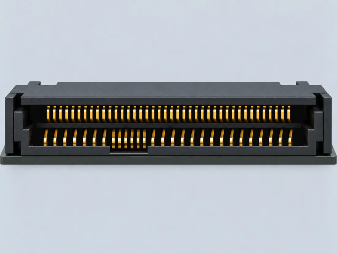
  • S777 · SNIA SFF TA TWG · SFF-8639: Multifunction 6X Unshielded Connector

    Rev 2.2, May 6, 2024 · p. 22 section 6.1 and Figure 6-1 Contact Numbering Scheme; p. 15 Figure 5-1 Device Free (Plug) Connector

Seagate Nytro 5060 2.5-inch U.2 device (named model family)

Device-specific wiring. Check your device’s manual before connecting or applying power.

View and evidence limits

Device manual Table 23 contact numbers. SG1/SG2 are separate ground features and are not counted among the 68 P/S/E contacts.

  • P198 U.2 / U.3 — **Agree** on comparable PCIe lane placement; **partial for sidebands/modes** — Both read **the same SFF-TA-1001 rev 1.1 and SFF-9639 rev 2.2 documents**, with matching hashes. U.3 PCIe-device assignments and the same 11 blank cells agree. U.2 puts lane 0 on E10/E11/E13/E14 and lane 3 on E17/E18/E20/E21; U.3 relocates PCIe lanes to S2-S27. A adds Wilder's U.2 test fixture; B adds Seagate Nytro 5060 and a separate U.3 universal-host column. Host/device E6 and S15, reserved versus fixture-defined HPT roles, and unused power/legacy-data contacts remain variant-specific. Shared SNIA evidence is not independent corroboration; Wilder and Seagate are additional, different device sources.
  • Device-specific implementation; do not use it as a universal U.2/U.3 replacement.
  • SFF-9639 expressly warns in section 5 that its tables are a reference guide and the using-interface specifications are definitive. Blank cells were not converted to NC/reserved. The PCI-SIG U.2 module specification was not obtained in this pass.
  • Only the explicit SFF-TA-1001 host/PCIe device columns and single-x4 numbering are mapped. SAS/SATA protocol-specific uses, dual-x2 remaps, Gen-Z and NVMe-oF are not silently combined into those variants; Tables 4-4/4-7 and SFF-9639 Table 6-1 must be followed for the selected mode.
U.2 / U.3 SFF-8639 68-position drive connector engineering referenceDevice manual Table 23 contact numbers. SG1/SG2 are separate ground features and are not counted among the 68 P/S/E contacts.SCHEMATIC · physical positions unconfirmedNot to scale · check the named wiring and device manualP1: Not confirmed (unverified)P1P2: Reserved (device_specific)P2P3: PWRDIS (device_specific)P3P4: IfDet# (device_specific)P4P5: Ground (device_specific)P5P6: Ground (device_specific)P6P7: NC (not_connected)P7P8: NC (not_connected)P8P9: NC (not_connected)P9P10: PRSNT# (device_specific)P10P11: ACTIVITY# (device_specific)P11P12: Ground (device_specific)P12P13: +12V Precharge (device_specific)P13P14: +12V (device_specific)P14P15: +12V (device_specific)P15S1: Ground (device_specific)S1S2: NC (not_connected)S2S3: NC (not_connected)S3S4: Ground (device_specific)S4S5: NC (not_connected)S5S6: NC (not_connected)S6S7: Ground (device_specific)S7S8: Ground (device_specific)S8S9: NC (not_connected)S9S10: NC (not_connected)S10S11: Ground (device_specific)S11S12: NC (not_connected)S12S13: NC (not_connected)S13S14: Ground (device_specific)S14S15: HPT0 (device_specific)S15S16: Ground (device_specific)S16S17: U.2 TX p1 (device_specific)S17S18: U.2 TX n1 (device_specific)S18S19: Ground (device_specific)S19S20: U.2 RX n1 (device_specific)S20S21: U.2 RX p1 (device_specific)S21S22: Ground (device_specific)S22S23: U.2 TX p2 (device_specific)S23S24: U.2 TX n2 (device_specific)S24S25: Ground (device_specific)S25S26: U.2 RX n2 (device_specific)S26S27: U.2 RX p2 (device_specific)S27S28: Ground (device_specific)S28E1: REFCLKB+ (device_specific)E1E2: REFCLKB- (device_specific)E2E3: +3.3Vaux (device_specific)E3E4: CLKREQ#/PERSTB# (device_specific)E4E5: PERST# (device_specific)E5E6: IFDet2# (device_specific)E6E7: REFCLK+ (device_specific)E7E8: REFCLK- (device_specific)E8E9: Ground (device_specific)E9E10: U.2 TX p0 (device_specific)E10E11: U.2 TX n0 (device_specific)E11E12: Ground (device_specific)E12E13: U.2 RX n0 (device_specific)E13E14: U.2 RX p0 (device_specific)E14E15: Ground (device_specific)E15E16: HPT1 (device_specific)E16E17: U.2 TX p3 (device_specific)E17E18: U.2 TX n3 (device_specific)E18E19: Ground (device_specific)E19E20: U.2 RX n3 (device_specific)E20E21: U.2 RX p3 (device_specific)E21E22: Ground (device_specific)E22E23: SMBCLK (device_specific)E23E24: SMBDAT (device_specific)E24E25: DualPortEn# (device_specific)E25powergrounddataConfigshieldNCUnknown
Schematic only · physical contact positions unconfirmed. Original drawing · not to scale. Scroll sideways if needed.
Seagate Nytro 5060 2.5-inch U.2 device (named model family) — source-scoped contact map
PinSignalWhat it doesStatus
P1Not confirmedNo settled assignment. Do not wire from this row.Unverified
Sources
P2ReservedReserved; no general-purpose wiring is established.Device-specific
Sources
P3PWRDISControl, detection or configuration connection; check the source and device.Device-specific
Sources
P4IfDet#Control, detection or configuration connection; check the source and device.Device-specific
Sources
P5GroundGround reference and return.Device-specific
Sources
P6GroundGround reference and return.Device-specific
Sources
P7NCNot connected or absent in this named wiring.Not connected
Sources
P8NCNot connected or absent in this named wiring.Not connected
Sources
P9NCNot connected or absent in this named wiring.Not connected
Sources
P10PRSNT#Control, detection or configuration connection; check the source and device.Device-specific
Sources
P11ACTIVITY#Control, detection or configuration connection; check the source and device.Device-specific
Sources
P12GroundGround reference and return.Device-specific
Sources
P13+12V PrechargePower connection (+12V Precharge). Check the specified supply.Device-specific
Sources
P14+12VPower connection (+12V). Check the specified supply.Device-specific
Sources
P15+12VPower connection (+12V). Check the specified supply.Device-specific
Sources
S1GroundGround reference and return.Device-specific
Sources
S2NCNot connected or absent in this named wiring.Not connected
Sources
S3NCNot connected or absent in this named wiring.Not connected
Sources
S4GroundGround reference and return.Device-specific
Sources
S5NCNot connected or absent in this named wiring.Not connected
Sources
S6NCNot connected or absent in this named wiring.Not connected
Sources
S7GroundGround reference and return.Device-specific
Sources
S8GroundGround reference and return.Device-specific
Sources
S9NCNot connected or absent in this named wiring.Not connected
Sources
S10NCNot connected or absent in this named wiring.Not connected
Sources
S11GroundGround reference and return.Device-specific
Sources
S12NCNot connected or absent in this named wiring.Not connected
Sources
S13NCNot connected or absent in this named wiring.Not connected
Sources
S14GroundGround reference and return.Device-specific
Sources
S15HPT0Control, detection or configuration connection; check the source and device.Device-specific
Sources
S16GroundGround reference and return.Device-specific
Sources
S17U.2 TX p1Signal conductor. Pair, polarity and direction follow this named wiring.Device-specific
Sources
S18U.2 TX n1Signal conductor. Pair, polarity and direction follow this named wiring.Device-specific
Sources
S19GroundGround reference and return.Device-specific
Sources
S20U.2 RX n1Signal conductor. Pair, polarity and direction follow this named wiring.Device-specific
Sources
S21U.2 RX p1Signal conductor. Pair, polarity and direction follow this named wiring.Device-specific
Sources
S22GroundGround reference and return.Device-specific
Sources
S23U.2 TX p2Signal conductor. Pair, polarity and direction follow this named wiring.Device-specific
Sources
S24U.2 TX n2Signal conductor. Pair, polarity and direction follow this named wiring.Device-specific
Sources
S25GroundGround reference and return.Device-specific
Sources
S26U.2 RX n2Signal conductor. Pair, polarity and direction follow this named wiring.Device-specific
Sources
S27U.2 RX p2Signal conductor. Pair, polarity and direction follow this named wiring.Device-specific
Sources
S28GroundGround reference and return.Device-specific
Sources
E1REFCLKB+Clock or clock-control connection, as named by this source.Device-specific
Sources
E2REFCLKB-Clock or clock-control connection, as named by this source.Device-specific
Sources
E3+3.3VauxPower connection (+3.3Vaux). Check the specified supply.Device-specific
Sources
E4CLKREQ#/PERSTB#Reset control; check active level and the named device.Device-specific
Sources
E5PERST#Reset control; check active level and the named device.Device-specific
Sources
E6IFDet2#Control, detection or configuration connection; check the source and device.Device-specific
Sources
E7REFCLK+Clock or clock-control connection, as named by this source.Device-specific
Sources
E8REFCLK-Clock or clock-control connection, as named by this source.Device-specific
Sources
E9GroundGround reference and return.Device-specific
Sources
E10U.2 TX p0Signal conductor. Pair, polarity and direction follow this named wiring.Device-specific
Sources
E11U.2 TX n0Signal conductor. Pair, polarity and direction follow this named wiring.Device-specific
Sources
E12GroundGround reference and return.Device-specific
Sources
E13U.2 RX n0Signal conductor. Pair, polarity and direction follow this named wiring.Device-specific
Sources
E14U.2 RX p0Signal conductor. Pair, polarity and direction follow this named wiring.Device-specific
Sources
E15GroundGround reference and return.Device-specific
Sources
E16HPT1Control, detection or configuration connection; check the source and device.Device-specific
Sources
E17U.2 TX p3Signal conductor. Pair, polarity and direction follow this named wiring.Device-specific
Sources
E18U.2 TX n3Signal conductor. Pair, polarity and direction follow this named wiring.Device-specific
Sources
E19GroundGround reference and return.Device-specific
Sources
E20U.2 RX n3Signal conductor. Pair, polarity and direction follow this named wiring.Device-specific
Sources
E21U.2 RX p3Signal conductor. Pair, polarity and direction follow this named wiring.Device-specific
Sources
E22GroundGround reference and return.Device-specific
Sources
E23SMBCLKClock or clock-control connection, as named by this source.Device-specific
Sources
E24SMBDATControl, detection or configuration connection; check the source and device.Device-specific
Sources
E25DualPortEn#Control, detection or configuration connection; check the source and device.Device-specific
Sources
Sources (2)
  • S778 · Seagate Technology LLC · Nytro 5060 NVMe 2.5-inch SSD Product Manual

    208169400, Rev B, February 2025 · p. 52, section 9.5.5 Table 23 Connector SFF-8639 Pin Assignment and Descriptions, row P1; p. 52, section 9.5.5 Table 23 Connector SFF-8639 Pin Assignment and Descriptions, row P2; p. 52, section 9.5.5 Table 23 Connector SFF-8639 Pin Assignment and Descriptions, row P3; p. 52, section 9.5.5 Table 23 Connector SFF-8639 Pin Assignment and Descriptions, row P4; p. 52, section 9.5.5 Table 23 Connector SFF-8639 Pin Assignment and Descriptions, row P5; p. 52, section 9.5.5 Table 23 Connector SFF-8639 Pin Assignment and Descriptions, row P6; p. 52, section 9.5.5 Table 23 Connector SFF-8639 Pin Assignment and Descriptions, row P7; p. 52, section 9.5.5 Table 23 Connector SFF-8639 Pin Assignment and Descriptions, row P8; p. 52, section 9.5.5 Table 23 Connector SFF-8639 Pin Assignment and Descriptions, row P9; p. 52, section 9.5.5 Table 23 Connector SFF-8639 Pin Assignment and Descriptions, row P10; p. 52, section 9.5.5 Table 23 Connector SFF-8639 Pin Assignment and Descriptions, row P11; p. 52, section 9.5.5 Table 23 Connector SFF-8639 Pin Assignment and Descriptions, row P12; p. 52, section 9.5.5 Table 23 Connector SFF-8639 Pin Assignment and Descriptions, row P13; p. 52, section 9.5.5 Table 23 Connector SFF-8639 Pin Assignment and Descriptions, row P14; p. 52, section 9.5.5 Table 23 Connector SFF-8639 Pin Assignment and Descriptions, row P15; p. 52, section 9.5.5 Table 23 Connector SFF-8639 Pin Assignment and Descriptions, row S1; p. 52, section 9.5.5 Table 23 Connector SFF-8639 Pin Assignment and Descriptions, row S2; p. 52, section 9.5.5 Table 23 Connector SFF-8639 Pin Assignment and Descriptions, row S3; p. 52, section 9.5.5 Table 23 Connector SFF-8639 Pin Assignment and Descriptions, row S4; p. 52, section 9.5.5 Table 23 Connector SFF-8639 Pin Assignment and Descriptions, row S5; p. 52, section 9.5.5 Table 23 Connector SFF-8639 Pin Assignment and Descriptions, row S6; p. 52, section 9.5.5 Table 23 Connector SFF-8639 Pin Assignment and Descriptions, row S7; p. 52, section 9.5.5 Table 23 Connector SFF-8639 Pin Assignment and Descriptions, row S8; p. 52, section 9.5.5 Table 23 Connector SFF-8639 Pin Assignment and Descriptions, row S9; p. 52, section 9.5.5 Table 23 Connector SFF-8639 Pin Assignment and Descriptions, row S10; p. 52, section 9.5.5 Table 23 Connector SFF-8639 Pin Assignment and Descriptions, row S11; p. 52, section 9.5.5 Table 23 Connector SFF-8639 Pin Assignment and Descriptions, row S12; p. 52, section 9.5.5 Table 23 Connector SFF-8639 Pin Assignment and Descriptions, row S13; p. 52, section 9.5.5 Table 23 Connector SFF-8639 Pin Assignment and Descriptions, row S14; p. 52, section 9.5.5 Table 23 Connector SFF-8639 Pin Assignment and Descriptions, row S15; p. 52, section 9.5.5 Table 23 Connector SFF-8639 Pin Assignment and Descriptions, row S16; p. 52, section 9.5.5 Table 23 Connector SFF-8639 Pin Assignment and Descriptions, row S17; p. 52, section 9.5.5 Table 23 Connector SFF-8639 Pin Assignment and Descriptions, row S18; p. 52, section 9.5.5 Table 23 Connector SFF-8639 Pin Assignment and Descriptions, row S19; p. 52, section 9.5.5 Table 23 Connector SFF-8639 Pin Assignment and Descriptions, row S20; p. 53, section 9.5.5 Table 23 Connector SFF-8639 Pin Assignment and Descriptions, row S21; p. 53, section 9.5.5 Table 23 Connector SFF-8639 Pin Assignment and Descriptions, row S22; p. 53, section 9.5.5 Table 23 Connector SFF-8639 Pin Assignment and Descriptions, row S23; p. 53, section 9.5.5 Table 23 Connector SFF-8639 Pin Assignment and Descriptions, row S24; p. 53, section 9.5.5 Table 23 Connector SFF-8639 Pin Assignment and Descriptions, row S25; p. 53, section 9.5.5 Table 23 Connector SFF-8639 Pin Assignment and Descriptions, row S26; p. 53, section 9.5.5 Table 23 Connector SFF-8639 Pin Assignment and Descriptions, row S27; p. 53, section 9.5.5 Table 23 Connector SFF-8639 Pin Assignment and Descriptions, row S28; p. 53, section 9.5.5 Table 23 Connector SFF-8639 Pin Assignment and Descriptions, row E1; p. 53, section 9.5.5 Table 23 Connector SFF-8639 Pin Assignment and Descriptions, row E2; p. 53, section 9.5.5 Table 23 Connector SFF-8639 Pin Assignment and Descriptions, row E3; p. 53, section 9.5.5 Table 23 Connector SFF-8639 Pin Assignment and Descriptions, row E4; p. 53, section 9.5.5 Table 23 Connector SFF-8639 Pin Assignment and Descriptions, row E5; p. 53, section 9.5.5 Table 23 Connector SFF-8639 Pin Assignment and Descriptions, row E6; p. 53, section 9.5.5 Table 23 Connector SFF-8639 Pin Assignment and Descriptions, row E7; p. 53, section 9.5.5 Table 23 Connector SFF-8639 Pin Assignment and Descriptions, row E8; p. 53, section 9.5.5 Table 23 Connector SFF-8639 Pin Assignment and Descriptions, row E9; p. 53, section 9.5.5 Table 23 Connector SFF-8639 Pin Assignment and Descriptions, row E10; p. 53, section 9.5.5 Table 23 Connector SFF-8639 Pin Assignment and Descriptions, row E11; p. 53, section 9.5.5 Table 23 Connector SFF-8639 Pin Assignment and Descriptions, row E12; p. 53, section 9.5.5 Table 23 Connector SFF-8639 Pin Assignment and Descriptions, row E13; p. 53, section 9.5.5 Table 23 Connector SFF-8639 Pin Assignment and Descriptions, row E14; p. 53, section 9.5.5 Table 23 Connector SFF-8639 Pin Assignment and Descriptions, row E15; p. 53, section 9.5.5 Table 23 Connector SFF-8639 Pin Assignment and Descriptions, row E16; p. 53, section 9.5.5 Table 23 Connector SFF-8639 Pin Assignment and Descriptions, row E17; p. 53, section 9.5.5 Table 23 Connector SFF-8639 Pin Assignment and Descriptions, row E18; p. 53, section 9.5.5 Table 23 Connector SFF-8639 Pin Assignment and Descriptions, row E19; p. 53, section 9.5.5 Table 23 Connector SFF-8639 Pin Assignment and Descriptions, row E20; p. 53, section 9.5.5 Table 23 Connector SFF-8639 Pin Assignment and Descriptions, row E21; p. 53, section 9.5.5 Table 23 Connector SFF-8639 Pin Assignment and Descriptions, row E22; p. 53, section 9.5.5 Table 23 Connector SFF-8639 Pin Assignment and Descriptions, row E23; p. 53, section 9.5.5 Table 23 Connector SFF-8639 Pin Assignment and Descriptions, row E24; p. 53, section 9.5.5 Table 23 Connector SFF-8639 Pin Assignment and Descriptions, row E25

  • S777 · SNIA SFF TA TWG · SFF-8639: Multifunction 6X Unshielded Connector

    Rev 2.2, May 6, 2024 · p. 22 section 6.1 and Figure 6-1 Contact Numbering Scheme; p. 15 Figure 5-1 Device Free (Plug) Connector

What is not established

This field note does not approve a connection, adapter, cable assembly, rewiring scheme or fabricated part. It intentionally omits unsupported pin assignments and mechanical tolerances.

Storage recognition: next evidence check

Match the exact drive, backplane, controller and cable to the applicable interface documentation. Keep U.2 and U.3 routing questions open until then. The exterior alone does not identify U.2 versus U.3, certify lane routing or authorize an adapter or live connection. Sources: C198B, C198C, C198D, C198E. Original qualitative study; independent technical and rights review pending.

Your next step

Move from the form to the requirement.

The source trail

Evidence for this page

AI-assisted inspection is not independent engineering review. Source scope and access limitations are disclosed below. Procedural checklists are editorial requirements, not hardware measurements.

Back to first citation ↑
C198ASource checked · pending review

Amphenol identifies its SAS/PCIe U.2/U.3 connector series as a 68-position interface compatible with SFF-8639.

Amphenol Communications Solutions · SAS/PCIe 5.0 U.2/U.3 connector series ↗

Locator: U.2/U.3 series overview
Access: public page. Identification/reference scope only. V36 does not convert this source into a universal pinout, fabrication drawing, electrical approval or end-to-end compatibility verdict.

S202: full source recordInspect review dependencies → (private workspace)

Claim scope: V36 catalogue-expansion identification fact only; not independent technical approval, fabrication data, wiring instruction or end-to-end compatibility proof.. Next review due 2027-01-03.

Back to first citation ↑
C198BSource checked · pending review

SFF-TA-8639 revision 2.2 defines a 68-contact system, while SFF-9639 explains that a device plug may populate only the contacts required by its use case.

SNIA · SNIA SFF-TA-8639 Multifunction 6X Unshielded Connector, revision 2.2 ↗

Locator: Rev 2.2, 2024-05-06. Sections 4.1 and 5.2; printed pp.15–16 Figures 5-1/5-2 visually inspected (PDF indices 14–15).
Access: public pdf text. No exact commercial component, U.2/U.3 system identification, signal routing, supported speed or live-mating approval established.

S599: full source recordSNIA · SNIA SFF-9639 Multifunction 6X connector reference guide, revision 2.2 ↗

Locator: Rev 2.2, May 2, 2025. Page 5 section 1.1 and page 7 section 5 including the source-authority warning; page 7 visually inspected.
Access: public pdf text. Not a definitive current pinout. This guide explicitly warns that its tables can lag the interface standards; tables are not reproduced.

S600: full source recordInspect review dependencies → (private workspace)

Claim scope: V143: the named drawing/revision or exact product page only. Recognition and document-role evidence; not a pinout, adapter verdict, dimensioned mating gauge, electrical approval or current installed-device claim.. Next review due 2027-01-11.

Back to first citation ↑
C198CSource checked · pending review

The device plug in SFF-TA-8639 Figure 5-1 has contact areas on opposite faces and additional fine-contact regions; one front-facing photograph cannot show the whole interface.

SNIA · SNIA SFF-TA-8639 Multifunction 6X Unshielded Connector, revision 2.2 ↗

Locator: Rev 2.2, 2024-05-06. Sections 4.1 and 5.2; printed pp.15–16 Figures 5-1/5-2 visually inspected (PDF indices 14–15).
Access: public pdf text. No exact commercial component, U.2/U.3 system identification, signal routing, supported speed or live-mating approval established.

S599: full source recordInspect review dependencies → (private workspace)

Claim scope: V143: the named drawing/revision or exact product page only. Recognition and document-role evidence; not a pinout, adapter verdict, dimensioned mating gauge, electrical approval or current installed-device claim.. Next review due 2027-01-11.

Back to first citation ↑
C198DSource checked · pending review

SFF-TA-8639 revision 2.2 section 5.2 says its fixed-connector footprint is not generally a replacement for SFF-8482 or SFF-8630 footprints.

SNIA · SNIA SFF-TA-8639 Multifunction 6X Unshielded Connector, revision 2.2 ↗

Locator: Rev 2.2, 2024-05-06. Sections 4.1 and 5.2; printed pp.15–16 Figures 5-1/5-2 visually inspected (PDF indices 14–15).
Access: public pdf text. No exact commercial component, U.2/U.3 system identification, signal routing, supported speed or live-mating approval established.

S599: full source recordInspect review dependencies → (private workspace)

Claim scope: V143: the named drawing/revision or exact product page only. Recognition and document-role evidence; not a pinout, adapter verdict, dimensioned mating gauge, electrical approval or current installed-device claim.. Next review due 2027-01-11.

Back to first citation ↑
C198ESource checked · pending review

SFF-9639 revision 2.2 is informational and directs readers to the using-interface standards for definitive signal definitions; it warns that its own tables may become inaccurate.

SNIA · SNIA SFF-9639 Multifunction 6X connector reference guide, revision 2.2 ↗

Locator: Rev 2.2, May 2, 2025. Page 5 section 1.1 and page 7 section 5 including the source-authority warning; page 7 visually inspected.
Access: public pdf text. Not a definitive current pinout. This guide explicitly warns that its tables can lag the interface standards; tables are not reproduced.

S600: full source recordInspect review dependencies → (private workspace)

Claim scope: V143: the named drawing/revision or exact product page only. Recognition and document-role evidence; not a pinout, adapter verdict, dimensioned mating gauge, electrical approval or current installed-device claim.. Next review due 2027-01-11.

Suggest a correction to this field note →

Put this field note to work.

Add to discovery trayRecord an unsaved candidate (private workspace)

Candidate selection does not confirm the identity or capabilities of your physical item.

Evidence behind this page

Scope first. Source second. Approval separate.

3 linked sources · 5 scoped claims · 0 sources with inspection/access flags.

Page scope: catalogue_expansion_v36

Assessment 2026-10-22 · earliest scheduled source review 2027-01-03. This is a recorded-date assessment, not a live source check. Page-level independent review is not established by this panel.

Inspect 3 source scopes, access limits and dates

S202 · SAS/PCIe 5.0 U.2/U.3 connector series

Amphenol Communications Solutions · Manufacturer / product-owner domain · inspected 2026-10-05 · due 2027-01-03

Within inspection window

Scoped support: Identifies a 68-position SAS/PCIe U.2/U.3 connector series compatible with the SFF-8639 interface family.

Not established / limitations: Identification/reference scope only. V36 does not convert this source into a universal pinout, fabrication drawing, electrical approval or end-to-end compatibility verdict.

Locator: U.2/U.3 series overview

S599 · SNIA SFF-TA-8639 Multifunction 6X Unshielded Connector, revision 2.2

SNIA · Standards-organization domain · inspected 2026-10-13 · due 2027-01-11

Within inspection window

Scoped support: 68-contact specification-interface device plug, opposing contact faces and footprint limitations.

Not established / limitations: No exact commercial component, U.2/U.3 system identification, signal routing, supported speed or live-mating approval established.

Locator: Rev 2.2, 2024-05-06. Sections 4.1 and 5.2; printed pp.15–16 Figures 5-1/5-2 visually inspected (PDF indices 14–15).

S600 · SNIA SFF-9639 Multifunction 6X connector reference guide, revision 2.2

SNIA · Standards-organization domain · inspected 2026-10-13 · due 2027-01-11

Within inspection window

Scoped support: Informational guide versus authoritative using-interface standards; contact population depends on use case.

Not established / limitations: Not a definitive current pinout. This guide explicitly warns that its tables can lag the interface standards; tables are not reproduced.

Locator: Rev 2.2, May 2, 2025. Page 5 section 1.1 and page 7 section 5 including the source-authority warning; page 7 visually inspected.

Trace 5 claims to their source records

C198A · P198

Amphenol identifies its SAS/PCIe U.2/U.3 connector series as a 68-position interface compatible with SFF-8639.

Claim scope: V36 catalogue-expansion identification fact only; not independent technical approval, fabrication data, wiring instruction or end-to-end compatibility proof.

Source links: S202 · Evidence trail → (private workspace)

C198B · P198

SFF-TA-8639 revision 2.2 defines a 68-contact system, while SFF-9639 explains that a device plug may populate only the contacts required by its use case.

Claim scope: V143: the named drawing/revision or exact product page only. Recognition and document-role evidence; not a pinout, adapter verdict, dimensioned mating gauge, electrical approval or current installed-device claim.

Source links: S599 · S600 · Evidence trail → (private workspace)

C198C · P198

The device plug in SFF-TA-8639 Figure 5-1 has contact areas on opposite faces and additional fine-contact regions; one front-facing photograph cannot show the whole interface.

Claim scope: V143: the named drawing/revision or exact product page only. Recognition and document-role evidence; not a pinout, adapter verdict, dimensioned mating gauge, electrical approval or current installed-device claim.

Source links: S599 · Evidence trail → (private workspace)

C198D · P198

SFF-TA-8639 revision 2.2 section 5.2 says its fixed-connector footprint is not generally a replacement for SFF-8482 or SFF-8630 footprints.

Claim scope: V143: the named drawing/revision or exact product page only. Recognition and document-role evidence; not a pinout, adapter verdict, dimensioned mating gauge, electrical approval or current installed-device claim.

Source links: S599 · Evidence trail → (private workspace)

C198E · P198

SFF-9639 revision 2.2 is informational and directs readers to the using-interface standards for definitive signal definitions; it warns that its own tables may become inaccurate.

Claim scope: V143: the named drawing/revision or exact product page only. Recognition and document-role evidence; not a pinout, adapter verdict, dimensioned mating gauge, electrical approval or current installed-device claim.

Source links: S600 · Evidence trail → (private workspace)

Prepare this page for review → (private workspace)Read the evidence method →

Recorded evidence only. An inspection date, publisher label, source link or generated packet is not independent technical review, hardware testing, fabrication approval or a compatibility verdict.